

Page 1

DISCRETE SEMICONDUCTORS
DATA SH EET
BLV90
UHF power transistor
Product specification
February 1996
Page 2
Philips Semiconductors Product specification
UHF power transistor BLV90
DESCRIPTION
NPN silicon planar epitaxial transistor designed for use in
mobile radio transmitters in the 900 MHz band.
FEATURES
• diffused emitter-ballasting resistors for an optimum
temperature profile.
• gold metallization ensures excellent reliability.
• the device can be applied at rated output power without
an external heatsink when it is mounted on a
printed-circuit board (see Fig.6).
The transistor has a 4-lead envelope with a ceramic cap
(SOT-172D). All leads are isolated from the mounting
base.
QUICK REFERENCE DATA
RF performance at T
a
MODE OF OPERATION
=25°C in a common-emitter class-B circuit.
V
CE
V
f
MHz
(1)
P
W
L
G
p
dB
η
%
Narrow band; CW 12.5 900 1 > 7.5 > 50
9.6 900 1 typ. 7.0 typ. 57
Note
1. Device mounted on a printed-circuit board (see Fig.6).
C
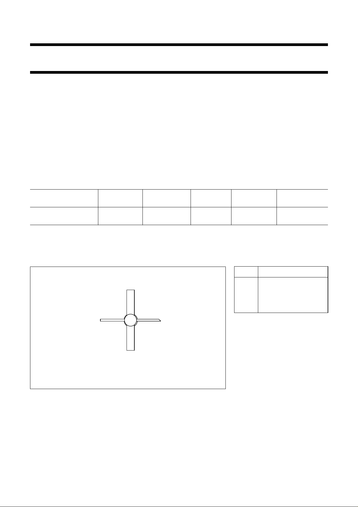
PIN CONFIGURATION
PINNING - SOT172D.
PIN DESCRIPTION
1 emitter
handbook, halfpage
1
2 base
3 collector
4 emitter
2
4
Top view
3
MSB007
Fig.1 Simplified outline. SOT172D.
PRODUCT SAFETY This device incorporates beryllium oxide, the dust of which is toxic. The device is entirely
safe provided that the BeO disc is not damaged.
February 1996 2
Page 3
Philips Semiconductors Product specification
UHF power transistor BLV90
RATINGS
Limiting values in accordance with the Absolute Maximum System (IEC 134)
Collector-base voltage (open emitter) V
Collector-emitter voltage (open base) V
Emitter-base voltage (open collector) V
CBO
CEO
EBO
Collector current
DC or average I
(peak value); f > 1 MHz I
C
CM
; I
C(AV)
Total power dissipation
f > 1 MHz; Tmb< 105 °CP
Storage temperature T
Operating junction temperature T
tot(rf)
stg
j
max. 36 V
max. 16 V
max. 3 V
max. 0.2 A
max. 0.6 A
max. 3.5 W
−65 to + 150 °C
max. 200 °C
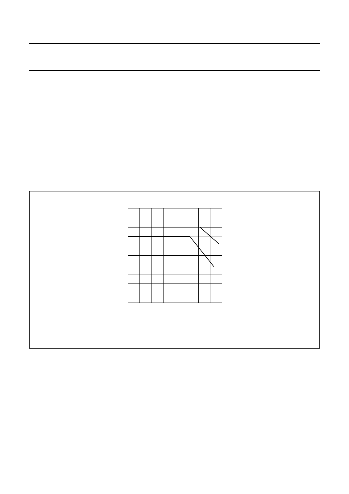
120
MDA389
Tmb (°C)
160
P
tot(rf)
(W)
5
4
3
2
1
0
0
handbook, halfpage
I Continuous RF operation (f > 1 MHz)
II Short-time RF operation during mismatch (f > 1 MHz)
II
I
40 80
Fig.2 Power/temperature curve.
THERMAL RESISTANCE
Dissipation = 2.25 W
From junction to ambient
T
=25°CR
a
(1)
(f > 1 MHz)
th j−a (RF)
max. 60 K/W
From junction to mounting base
T
=25°C(f>1 MHz) R
mb
th j-mb (RF)
max. 19 K/W
Note
1. Device mounted on a printed-circuit board (see Fig.6).
February 1996 3
Page 4

Philips Semiconductors Product specification
UHF power transistor BLV90
CHARACTERISTICS
T
=25°C unless otherwise specified
j
Collector-base breakdown voltage
open emitter; I
Collector-emitter breakdown voltage
open base; IC= 10 mA V
Emitter-base breakdown voltage
open collector; IE= 0.5 mA V
Collector cut-off current
VBE= 0; VCE= 16 V I
Second breakdown energy
L = 25 mH; f = 50 Hz; R
D.C. current gain
I
= 0.15 A; VCE= 10 V h
C
Collector capacitance at f = 1 MHz
I
= 0; VCB= 12.5 V C
E=ie
Feedback capacitance at f = 1 MHz
I
= 0; VCE= 12.5 V C
C
Collector-mounting base capacitance C
= 2.5 mA V
C
=10Ω E
BE
(BR)CBO
(BR)CEO
(BR)EBO
CES
SBR
FE
c
re
c-mb
> 36 V
> 16 V
> 3V
< 1mA
> 0.3 mJ
> 25
typ. 1.8 pF
typ. 1.0 pF
typ. 0.5 pF
120
handbook, halfpage
h
FE
80
40
0
0
V
12.5 V
10 V
150
300 600450
IC (mA)
Fig.3 Tj=25°C; typical values.
MDA390
CE
12
V
CB
MDA391
(V)
16
handbook, halfpage
=
4
C
c
(pF)
3
2
1
0
048
Fig.4 IE=ie= 0; f = 1 MHz; typical values.
February 1996 4
Page 5

Philips Semiconductors Product specification
UHF power transistor BLV90
APPLICATION INFORMATION
RF performance in CW operation (common-emitter circuit, class-B): f = 900 MHz; T
=25°C
a
MODE OF OPERATION
V
CE
V
P
L
W
G
dB
p
η
C
%
narrow band; CW 12.5 1 > 7.5 > 50
typ. 9.0 typ. 60
9.6 1 typ. 7.0 typ. 57
handbook, full pagewidth
R1
C1
L8
L2
C2
C4
L1
C3 C8
T.U.T.
L3
L4
C5 C6
L5
L9
R2
C7
L6 L7
MDA392
C9
+V
CC
C10
Fig.5 Class-B test circuit at f = 900 MHz.
List of components:
C1 = C10 = 33 pF multilayer ceramic chip capacitor
C2 = C9 = 1.4 to 5.5 pF film dielectric trimmer (cat. no. 2222 809 09001)
C3 = 2 to 9 pF film dielectric trimmer (cat. no. 2222 809 09002)
C4 = 5.6 pF multilayer ceramic chip capacitor
(1)
C5 = 10 pF multilayer ceramic chip capacitor
C6 = 330 pF multilayer ceramic chip capacitor
C7 = 3.9 pF multilayer ceramic chip capacitor
(1)
C8 = 1.2 to 3.5 pF film dielectric trimmer (cat. no. 2222 809 05001)
L1 = L7 = 50 Ω stripline (30.8 mm × 2.4 mm)
L2 = 60 nH; 4 turns closely wound enamelled Cu wire (0.4 mm); int. dia. 3 mm; leads 2 × 5 mm
L3 = 38 Ω stripline (16.0 mm × 3.5 mm)
L4 = 38 Ω stripline (11.0 mm × 3.5 mm)
L5 = 280 nH; 15 turns closely wound enamelled Cu wire (0.4 mm); int. dia. 3 mm; leads 2 × 5 mm
L6 = 50 Ω stripline (41.2 mm × 2.4 mm)
L8 = L9 = Ferroxcube wideband HF choke, grade 3B (cat. no. 4312 020 36642)
R1 = R2 = 10 Ω ± 5%; 0.25 W metal film resistor
L1, L3, L4, L6 and L7 are striplines on a double Cu-clad printed-circuit board with P.T.F.E. fibre-glass dielectric
(ε
= 2.2); thickness1⁄32 inch; thickness of copper-sheet 2 × 35 µm.
r
50 Ω50 Ω
Notes
1. American Technical Ceramics capacitor type 100A or capacitor of same quality.
2. Device mounted on a printed-circuit board (see Fig.6).
February 1996 5
Page 6

Philips Semiconductors Product specification
UHF power transistor BLV90
handbook, full pagewidth
C1
L2
C2
copper straps
L8
R1
C3
160 mm
M2
C5
E
L4L3
BC
E
80 mm
rivets
+V
CC
L9
C6
R2
L5
C7
L6L1
C8 C9
L7
C10
The circuit and the components are on one side of the P.T.F.E. fibre-glass board; the other side
is unetched copper serving as groundplane. Earth connections are made by hollow rivets and
also by fixing-screws and copper straps around the board and under the emitters to provide a
direct contact between the copper on the component side and the groundplane.
Fig.6 Printed-circuit board and component lay-out for 900 MHz class-B test circuit.
February 1996 6
MDA393
Page 7

Philips Semiconductors Product specification
UHF power transistor BLV90
1.6
handbook, halfpage
P
L
(W)
1.2
0.8
0.4
0
0 0.1
f = 900 MHz; class-B operation; typical values.
Tmb= 25 °C; VCE= 12.5 V;
− − − − T
- - - - T
=25°C; VCE= 12.5 V;
a
=25°C; VCE= 9.6 V
a
0.2 0.3
MDA394
PS (W)
Fig.7 Load power as a function of source power.
1.2
MDA395
PL (W)
12
handbook, halfpage
G
p
(dB)
G
8
4
0
0
f = 900 MHz; class-B operation; typical values.
Tmb= 25 °C; VCE= 12.5 V;
− − − − T
a
=25°C; VCE= 9.6 V
- - - - T
a
p
η
C
0.4
=25°C; VCE= 12.5 V;
0.8 1.6
Fig.8 Power gain and efficiency as a function of
load power.
120
η
(%)
80
40
0
C
RUGGEDNESS
The device is capable to withstand a full load mismatch
(VSWR = 50; all phases) at rated load power up to a
supply voltage of 15.5 V at Ta=25°C. Device mounted on
a printed-circuit board (see Fig.6).
February 1996 7
Page 8

Philips Semiconductors Product specification
UHF power transistor BLV90
handbook, halfpage
8
Z
i
(Ω)
6
4
2
0
−2
800 1000
VCE= 12.5 V; PL= 1 W; f = 800 - 960 MHz;
=25°C; class-B operation; typical values.
T
mb
840
880 920
Fig.9 Input impedance (series components).
960
MDA396
r
i
x
i
f (MHz)
25
handbook, halfpage
Z
L
(Ω)
23
21
19
17
15
800 1000
VCE= 12.5 V; PL= 1 W; f = 800 - 960 MHz;
=25°C; class-B operation; typical values.
T
mb
840
880 920
960
Fig.10 Load impedance (series components).
MDA397
X
L
R
L
f (MHz)
950
MDA563
f (MHz)
12
handbook, halfpage
G
p
(dB)
8
4
0
800
VCE= 12.5 V; PL= 1 W; f = 800 - 960 MHz;
=25°C; class-B operation; typical values.
T
mb
850
900 1000
Fig.11 Power gain as a function of frequency.
February 1996 8
Page 9

Philips Semiconductors Product specification
UHF power transistor BLV90
PACKAGE OUTLINE
Studless ceramic package; 4 leads SOT172D
D
A
Q
D
1
H
b
c
4
b
1
H
1
2
0 5 10 mm
scale
DIMENSIONS (millimetre dimensions are derived from the original inch dimensions)
UNIT
mm
inches
A
3.71
2.89
0.146
0.114
3.31
3.04
0.13
0.12
0.035
0.025
b
0.89
0.63
c
Db
D
H
1
5.20
0.16
4.95
0.10
0.205
0.006
0.195
0.004
5.33
5.08
0.210
0.200
1
26.17
24.63
1.03
0.97
Q
1.15
0.88
0.045
0.035
3
OUTLINE
VERSION
SOT172D
IEC JEDEC EIAJ
REFERENCES
February 1996 9
EUROPEAN
PROJECTION
ISSUE DATE
97-06-28
Page 10

Philips Semiconductors Product specification
UHF power transistor BLV90
DEFINITIONS
Data Sheet Status
Objective specification This data sheet contains target or goal specifications for product development.
Preliminary specification This data sheet contains preliminary data; supplementary data may be published later.
Product specification This data sheet contains final product specifications.
Limiting values
Limiting values given are in accordance with the Absolute Maximum Rating System (IEC 134). Stress above one or
more of the limiting values may cause permanent damage to the device. These are stress ratings only and operation
of the device at these or at any other conditions above those given in the Characteristics sections of the specification
is not implied. Exposure to limiting values for extended periods may affect device reliability.
Application information
Where application information is given, it is advisory and does not form part of the specification.
LIFE SUPPORT APPLICATIONS
These products are not designed for use in life support appliances, devices, or systems where malfunction of these
products can reasonably be expected to result in personal injury. Philips customers using or selling these products for
use in such applications do so at their own risk and agree to fully indemnify Philips for any damages resulting from such
improper use or sale.
February 1996 10
 Loading...