

Page 1

DISCRETE SEMICONDUCTORS
DATA SH EET
BLV58
UHF linear push-pull power
transistor
Product specification
September 1991
Page 2
Philips Semiconductors Product specification
UHF linear push-pull power transistor BLV58
FEATURES
• High power gain
• Double stage internal input
matching for high input impedance
• Diffused emitter-ballasting resistors
enhances ruggedness
• Gold metallization for high
reliability.
DESCRIPTION
The BLV58 is a common emitter
epitaxial npn silicon planar transistor
designed for high linearity class-A
operation in UHF (bands 4 and 5) TV
transmitters and transposers.
The device is incorporated in a
push-pull SOT289 flange envelope
with a ceramic cap, which is utilized
with the emitters connected to the
flange.
PINNING - SOT289
QUICK REFERENCE DATA
RF performance at T
MODE OF
OPERATION
= 25 °C in a common emitter test circuit.
h
f
vision
(MHz)
V
(V)
CE
I
CQ
(A)
P
o sync
(W)
G
(dB)
p
d
(dB)
(note 1)
c.w. class-A 860 25 2 × 1.6 25 >10 <−45
Note
1. Three-tone test method (vision carrier −8 dB, sound carrier −7 dB,
sideband signal −16 dB); zero dB corresponds to peak sync level.
PIN CONFIGURATION
c1
, halfpage
12
34
Top view
5
MBC043
handbook, halfpage
b1
b2
MBA970
e
c2
im
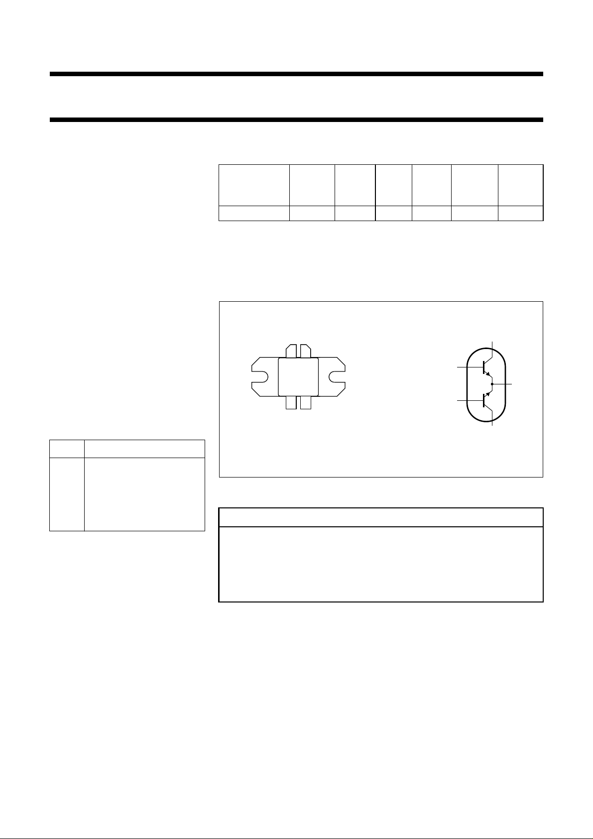
PIN DESCRIPTION
1 collector 1
2 collector 2
3 base 1
4 base 2
5 emitter
Fig.1 Simplified outline and symbol.
WARNING
Product and environmental safety - toxic materials
This product contains beryllium oxide. The product is entirely safe provided
that the BeO discs are not damaged. All persons who handle, use or dispose
of this product should be aware of its nature and of the necessary safety
precautions. After use, dispose of as chemical or special waste according to
the regulations applying at the location of the user. It must never be thrown
out with the general or domestic waste.
September 1991 2
Page 3
Philips Semiconductors Product specification
UHF linear push-pull power transistor BLV58
LIMITING VALUES (per transistor section unless otherwise specified)
In accordance with the Absolute Maximum System (IEC 134).
SYMBOL PARAMETER CONDITIONS MIN. MAX. UNIT
V
CBO
V
CEO
V
EBO
I
C,IC(AV)
I
CM
P
tot
T
stg
T
j
Note
1. Total device, both sections equally loaded.
collector-base voltage open emitter − 50 V
collector-emitter voltage open base − 27 V
emitter-base voltage open collector − 3.5 V
collector current DC or average value − 4A
collector current peak value;
− 8A
f > 1 MHz
total power dissipation DC operation;
− 87 W
Tmb=70°C
(note 1)
storage temperature range −65 150 °C
junction operating temperature − 200 °C
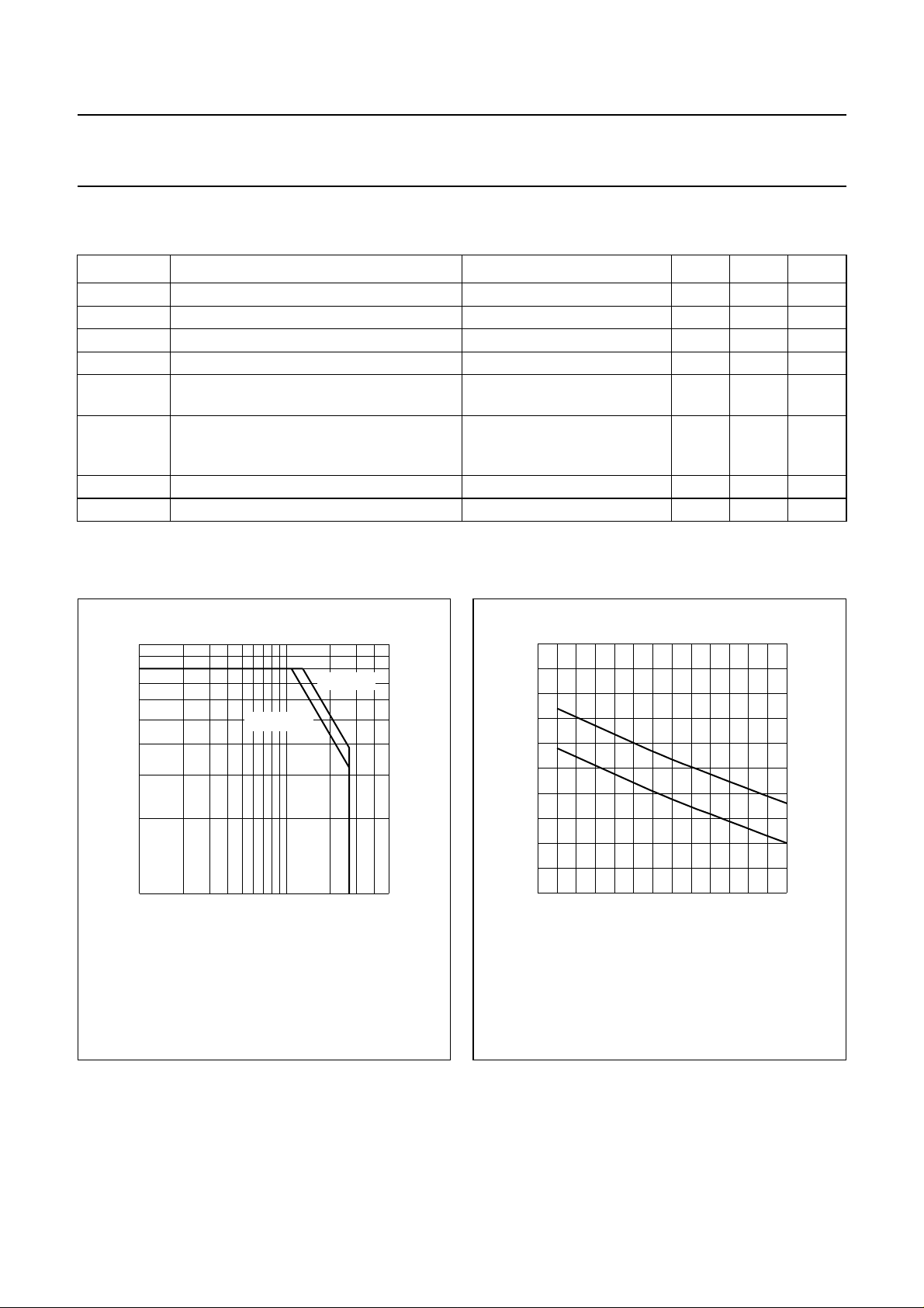
10
handbook, halfpage
I
C
(A)
T = 70 C
mb
1
110
Total device, both sections equally loaded.
Fig.2 DC SOAR.
o
T
= 25
h
C
V (V)
CE
MRA354
o
200
handbook, halfpage
P
tot
(W)
160
120
80
40
0
50
0 20 40 60 80 100 120
(I) Continuous DC operation.
(II) Short time operation during mismatch.
Total device, both sections equally loaded.
II
I
MRA355
T
h
o
( C)
Fig.3 Power derating curve.
September 1991 3
Page 4
Philips Semiconductors Product specification
UHF linear push-pull power transistor BLV58
THERMAL RESISTANCE
SYMBOL PARAMETER CONDITIONS MAX. UNIT
R
th j-mb(DC)
R
th mb-h
from junction to mounting base P
from mounting base to heatsink note 1 0.2 K/W
Note
1. Total device, both sections equally loaded.
CHARACTERISTICS
Values apply to either transistor section; T
= 25 °C.
j
SYMBOL PARAMETER CONDITIONS MIN. TYP. MAX. UNIT
V
(BR)CBO
collector-base breakdown voltage open emitter;
IC=20mA
V
(BR)CEO
collector-emitter breakdown voltage open base;
IC=50mA
V
(BR)EBO
emitter-base breakdown voltage open collector;
IE=10mA
I
CES
collector-emitter leakage current VBE=0;
VCE=27V
h
FE
DC current gain VCE=25V;
IC= 1.6 A
C
c
collector capacitance VCB=25V;
IE=Ie=0;
f=1MHz
=87W;
dis
Tmb=70°C
(note 1)
1.5 K/W
50 −− V
27 −− V
3.5 −− V
−−10 mA
30 −−
− 36 45 pF
September 1991 4
Page 5

Philips Semiconductors Product specification
UHF linear push-pull power transistor BLV58
C
MRA350
(A)I
120
handbook, halfpage
h
FE
80
40
0
0123
VCE=25V.
Fig.4 DC current gain as a function of collector
current, typical values.
handbook, halfpage
C
c
(pF)
120
80
40
0
0 10203040
IE=ie= 0; f= 1 MHz.
Fig.5 Collector capacitance as a function of
collector-base voltage, typical values.
MRA346
CB
(V)V
September 1991 5
Page 6

Philips Semiconductors Product specification
UHF linear push-pull power transistor BLV58
APPLICATION INFORMATION
RF performance at T
=25°C in a common emitter push-pull test circuit; R
h
th mb-h
= 0.2 K/W.
MODE OF OPERA TION
f
vision
(MHz)
V
(V)
CE
I
CQ
(A)
P
o sync
(W)
G
(dB)
c.w. class-A 860 25 2 × 1.6 25 > 10
typ. 11.5
d
P
im
(dB)
(note 1)
<−45
typ. −47
d
cm
(%)
(note 2)
< 20
Notes
1. Three-tone test method: vision carrier −8 dB (860 MHz), sound carrier −7 dB (865.5 MHz), sideband signal −16 dB
(861 MHz); zero dB corresponds to peak sync level.
2. Two-tone test method: vision carrier 0 dB (860 MHz), sound carrier−7 dB (865.5 MHz); zero dB corresponds to peak
sync level. Cross-modulation distortion (d
) is the voltage variation (%) of the sound carrier when the vision carrier
cm
is switched from 0 dB to −20 dB.
-40
handbook, halfpage
d
im
(dB)
-50
-60
o
T = 70 C
h
o
T = 25 C
h
MRA351
d
im
(dB)
-40
-42
-44
-46
-48
handbook, halfpage
T
= 25
h
C
o
T
h
o
= 70 C
MRA349
-70
0102030
Class-A operation; VCE= 25 V; f = 860 MHz; 3-tone test
(−8 dB, −16 dB, −7 dB); I
=2×1.6 A.
CQ
o sync
(W)P
Fig.6 Intermodulation distortion as a function of
output power.
Ruggedness in Class-A operation
The BLV58 is capable of withstanding a full load mismatch
corresponding to VSWR = 50:1 through all phases under
the following conditions:
September 1991 6
-50
1.6 2.4 3.2 4
Class-A operation; VCE= 25 V; f = 860 MHz; 3-tone test
(−8 dB, −16 dB, −7 dB); P
o sync
=25W.
I
(A)
C
Fig.7 Intermodulation distortion as a function of
collector current.
= 25 V, f = 860 MHz, Th=25°C,
V
CE
R
= 0.2 K/W, ICQ=2×1.6 A,
th mb-h
and rated output power.
Page 7

Philips Semiconductors Product specification
UHF linear push-pull power transistor BLV58
handbook, halfpage
P
o sync
(W)
30
20
10
0
0123
Class-A operation; VCE= 25 V; f = 860 MHz; 3-tone test
(−8 dB, −16 dB, −7 dB); I
CQ
o
T = 25 C
h
T = 70 C
=2×1.6 A.
h
MRA356
o
i sync
Fig.8 Output power as a function of input power.
13
handbook, halfpage
G
P
(dB)
11
9
7
(W)P
0102030
Class-A operation; VCE= 25 V; f = 860 MHz; 3-tone test
(−8 dB, −16 dB, −7 dB); I
o
T = 70 C
mb
=2×1.6 A.
CQ
o
T = 25 C
h
MRA348
P (W)
o sync
Fig.9 Gain as a function of output power, typical
values.
September 1991 7
Page 8

Philips Semiconductors Product specification
UHF linear push-pull power transistor BLV58
V
CC
C15
C16
50 Ω
input
V
BB
C7
C8
C9
C10
L6
C1
L1
L2
C3
L3
C2
L4
C5C4
L5
C11
C12
L8
C6
L9
L7
C13
C14
V
BB
BLV58
T.U.T.
L12 R1
C17
C18
C19
C20
C21
L13
L10
C29 C30 C33
L11 L17 L19
C22
C24
L15
L16 L18
C31
C32
C23
C25
C26
R2
C34
C35
L20
L21
L22
50 Ω
output
handbook, full pagewidth
Fig.10 Class-A test circuit at f = 860 MHz.
September 1991 8
C27
C28
V
CC
MBC048
Page 9

Philips Semiconductors Product specification
UHF linear push-pull power transistor BLV58
List of components (see test circuit)
COMPONENT DESCRIPTION VALUE DIMENSIONS CATALOGUE NO.
C1, C2, C34,
C35
C3 multilayer ceramic chip capacitor
C4, C6 film dielectric trimmer 5.5 pF 2222 809 09005
C5 multilayer ceramic chip capacitor
C7, C12, C17,
C26
C8, C14, C19,
C25
C9, C11, C16,
C20, C22, C28
C10, C13, C15,
C21, C23, C27
C18, C24 63 V electrolytic capacitor 1 µF
C29 multilayer ceramic chip capacitor
C30 multilayer ceramic chip capacitor
C31, C33 film dielectric trimmer 3.5 pF 2222 809 05001
C32 multilayer ceramic chip capacitor (note 1) 2.7 pF
L1, L3, L20, L22 stripline (note 2) 35 Ω 39 mm × 4mm
L2, L21 semi-rigid cable (note 3) 50 Ω ext. dia. 3.6 mm;
L4, L5 stripline (note 2) 38 Ω 19 mm × 3.5 mm
L6, L7 RF choke 470 nH
L8, L9 stripline (note 2) 38 Ω 7.5 mm × 3.5 mm
L10, L11 stripline (note 2) 38 Ω 4.5 mm × 3.5 mm
L12, L15 grade 3B RF choke 4312 020 36642
L13, L14 1 turn 1.5 mm copper wire 14 nH int. dia 7 mm;
L16, L17 stripline (note 2) 38 Ω 7mm× 3.5 mm
L18, L19 stripline (note 2) 38 Ω 18 mm × 3.5 mm
R1, R2 1 W metal film resistor 10 Ω
multilayer ceramic chip capacitor
(note 1)
(note 1)
(note 1)
multilayer ceramic chip capacitor 10 nF 2222 852 47103
multilayer ceramic chip capacitor 100 nF 2222 852 47104
63 V electrolytic capacitor 10 µF
multilayer ceramic chip capacitor
(note 1)
(note 1)
(note 1)
15 pF
3.9 pF
7.5 pF
330 pF
12 pF
5.6 pF
length 39 mm
leads 2 × 6mm
Notes
1. American Technical Ceramics type 100B or capacitor of the same quality.
2. The striplines are on a double copper-clad printed circuit board, with PTFE microfibre-glass dielectric (ε
thickness1⁄32inch, thickness of copper sheet 2 × 35 µm.
3. Cables L2 and L21 are soldered to striplines L1 and L20, respectively.
September 1991 9
= 2.2),
r
Page 10

Philips Semiconductors Product specification
UHF linear push-pull power transistor BLV58
handbook, full pagewidth
handbook, full pagewidth
L1
L2 + L3
C1
C2
C3
C4
170 mm
rivet
(2x)
copper strap
(6x)
MBC046
C7
C8
C9
C10
L6
L4
C5
C6
L5
L7
C14
C11
C13
C12
C18
C17
C19
C21
L10
L8
C29
L9
L11
C26
C25
C23
C22
L13
L16
L17
L14
L12
R1
R2
L15
C20
C30
C31
L19
C24
L18
C32
C33
C34
C35
C16
C15
C27
C28
L21 +
L22
L20
MBC047
80 mm
The components are mounted on one side of a copper clad PTFE microfibre-glass board; the other side is
unetched and serves as a ground plane. Earth connections from the component side to the ground plane are
made by hollow rivets and copper straps.
Fig.11 Component layout for 860 MHz class-A test circuit.
September 1991 10
Page 11

Philips Semiconductors Product specification
UHF linear push-pull power transistor BLV58
handbook, halfpage
6
Z
i
(Ω)
4
x
i
2
0
400 500 600 700 800 900
Class-A operation; VCE=25V;
= 1.6 A (per section); PL= 25 W (total device);
I
CQ
=25°C.
T
h
r
i
Fig.12 Input impedance per section (series
components) as a function of frequency,
typical values.
MRA352
f (MHz)
handbook, halfpage
6
Z
L
(Ω)
4
R
L
2
0
-1
400 500 600 700 800 900
Class-A operation; VCE=25V;
= 1.6 A (per section); PL= 25 W (total device);
I
CQ
=25°C.
T
h
X
L
Fig.13 Load impedance per section (series
components) as a function of frequency,
typical values.
MRA353
f (MHz)
handbook, halfpage
Fig.14 Definition of transistor impedance.
16
handbook, halfpage
G
P
(dB)
14
12
Z
i
Z
MBA451
L
10
400 500 600 700 800 900
Class-A operation; VCE=25V;
= 1.6 A (per section); PL= 25 W (total device);
I
CQ
=25°C.
T
h
MRA347
f (MHz)
Fig.15 Power gain as a function of frequency,
typical values.
September 1991 11
Page 12

Philips Semiconductors Product specification
UHF linear push-pull power transistor BLV58
PACKAGE OUTLINE
Flanged ceramic package; 2 mounting holes; 4 leads SOT289A
D
A
F
5
U
1
q
H
1
1
U2H
A
DIMENSIONS (millimetre dimensions are derived from the original inch dimensions)
3.33
3.07
c
0.10
0.05
0.004
0.002
Db
13.10
12.90
0.516
0.508
UNIT
mm
inches
A
4.65
3.92
0.183
0.154
0.131
0.121
3
b
e
F
e
EU
11.53
11.33
0.454
0.446
4.60
0.181
1.65
1.40
0.065
0.055
w
2
4
w
0 5 10 mm
scale
H
H
19.81
4.85
19.05
4.34
0.780
0.191
0.750
0.171
C
M
C
2
M
3
p
1
3.43
3.17
0.135
0.125
B
Q
2.31
2.06
0.091
0.081
c
p
w
M
AB
1
Q
qw
U
1
28.07
21.44
27.81
1.105
1.095
w
1
2
11.81
11.56
0.465
0.455
E
w
3
2
0.250.51 1.02
0.010.02 0.040.844
OUTLINE
VERSION
SOT289A 97-06-28
IEC JEDEC EIAJ
REFERENCES
EUROPEAN
PROJECTION
September 1991 12
ISSUE DATE
Page 13

Philips Semiconductors Product specification
UHF linear push-pull power transistor BLV58
DEFINITIONS
Data Sheet Status
Objective specification This data sheet contains target or goal specifications for product development.
Preliminary specification This data sheet contains preliminary data; supplementary data may be published later.
Product specification This data sheet contains final product specifications.
Limiting values
Limiting values given are in accordance with the Absolute Maximum Rating System (IEC 134). Stress above one or
more of the limiting values may cause permanent damage to the device. These are stress ratings only and operation
of the device at these or at any other conditions above those given in the Characteristics sections of the specification
is not implied. Exposure to limiting values for extended periods may affect device reliability.
Application information
Where application information is given, it is advisory and does not form part of the specification.
LIFE SUPPORT APPLICATIONS
These products are not designed for use in life support appliances, devices, or systems where malfunction of these
products can reasonably be expected to result in personal injury. Philips customers using or selling these products for
use in such applications do so at their own risk and agree to fully indemnify Philips for any damages resulting from such
improper use or sale.
September 1991 13
 Loading...