

Page 1

DISCRETE SEMICONDUCTORS
DATA SH EET
BLV33F
VHF linear power transistor
Product specification
1996 Oct 10
Page 2
Philips Semiconductors Product specification
VHF linear power transistor BLV33F
FEATURES
• Internally matched input for wideband operation and
high power gain
• Diffused emitter ballasting resistors for an optimum
temperature profile
• Gold metallization ensures excellent reliability.
APPLICATIONS
• Primarily intended for use in linear VHF amplifiers for
television transmitters and transposers.
DESCRIPTION
NPN silicon planar epitaxial transistor encapsulated in a
1
⁄2” 6 lead SOT119A capstan package with ceramic cap.
All leads are isolated from the flange.
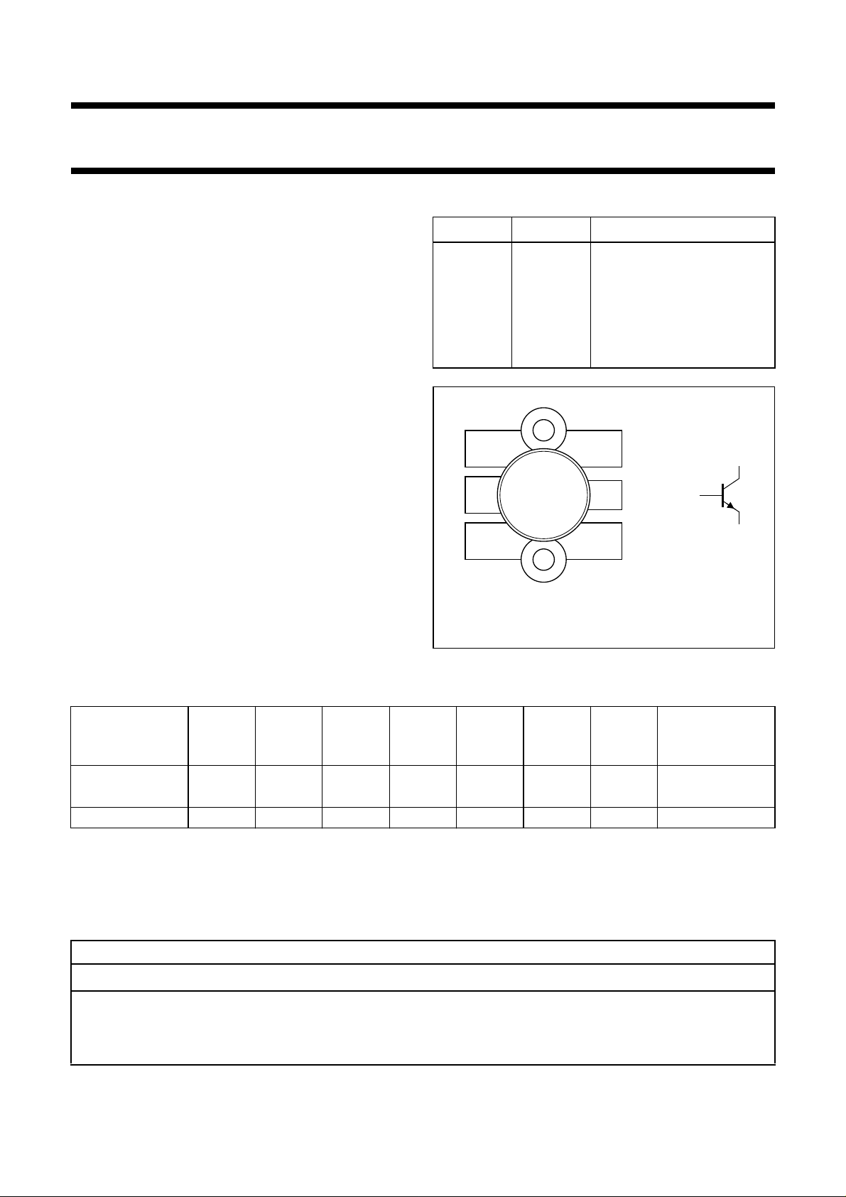
PINNING - SOT119A
PIN SYMBOL DESCRIPTION
1 e emitter
2 e emitter
3 b base
4 c collector
5 e emitter
6 e emitter
handbook, halfpage
1
3
2
4
65
c
b
e
MAM269
Fig.1 Simplified outline and symbol.
QUICK REFERENCE DATA
RF performance in a common emitter push-pull test circuit.
MODE OF
OPERATION
f
vision
(MHz)
V
(V)
CE
IC, I
(A)
CW, class-A 224.25 25 3.2
C(ZS)
T
(°C)
(1)
h
d
im
P
(dB)
o sync
(W)
(1)
G
P
(dB)
70 −55 >13 >13.5
25 −55 typ. 19 typ. 14.8
sync compr.
sync in/sync out
(%)
(2)
CW, class-AB 224.25 28 0.2 70 − typ. 85 typ. 10.5 30/25
Notes
1. Three-tone test method (vision carrier −8 dB, sound carrier −7 dB, sideband signal−16 dB), zero dB corresponds to
peak sync level.
2. Television service (negative modulation, C.C.I.R. system).
WARNING
Product and environmental safety - toxic materials
This product contains beryllium oxide. The product is entirely safe provided that the BeO disc is not damaged.
All persons who handle, use or dispose of this product should be aware of its nature and of the necessary safety
precautions. After use, dispose of as chemical or special waste according to the regulations applying at the location of
the user. It must never be thrown out with the general or domestic waste.
1996 Oct 10 2
Page 3
Philips Semiconductors Product specification
VHF linear power transistor BLV33F
LIMITING VALUES
In accordance with the Absolute Maximum Rating System (IEC 134).
SYMBOL PARAMETER CONDITIONS MIN. MAX. UNIT
V
CESM
V
CEO
V
EBO
I
C
I
C(AV)
I
CM
P
tot
P
rf
T
stg
T
j
THERMAL CHARACTERISTICS
collector-emitter voltage VBE=0 − 65 V
collector-emitter voltage open base − 33 V
emitter-base voltage open collector − 4V
collector current (DC) − 12.5 A
average collector current − 12.5 A
peak collector current f > 1 MHz − 20 A
total power dissipation (DC) Tmb=25°C − 133 W
RF power dissipation f > 1 MHz; Tmb=25°C − 162 W
storage temperature −65 +150 °C
operating junction temperature − 200 °C
SYMBOL PARAMETER CONDITIONS VALUE UNIT
R
th j-mb(dc)
R
th j-mb(rf)
R
th mb-h
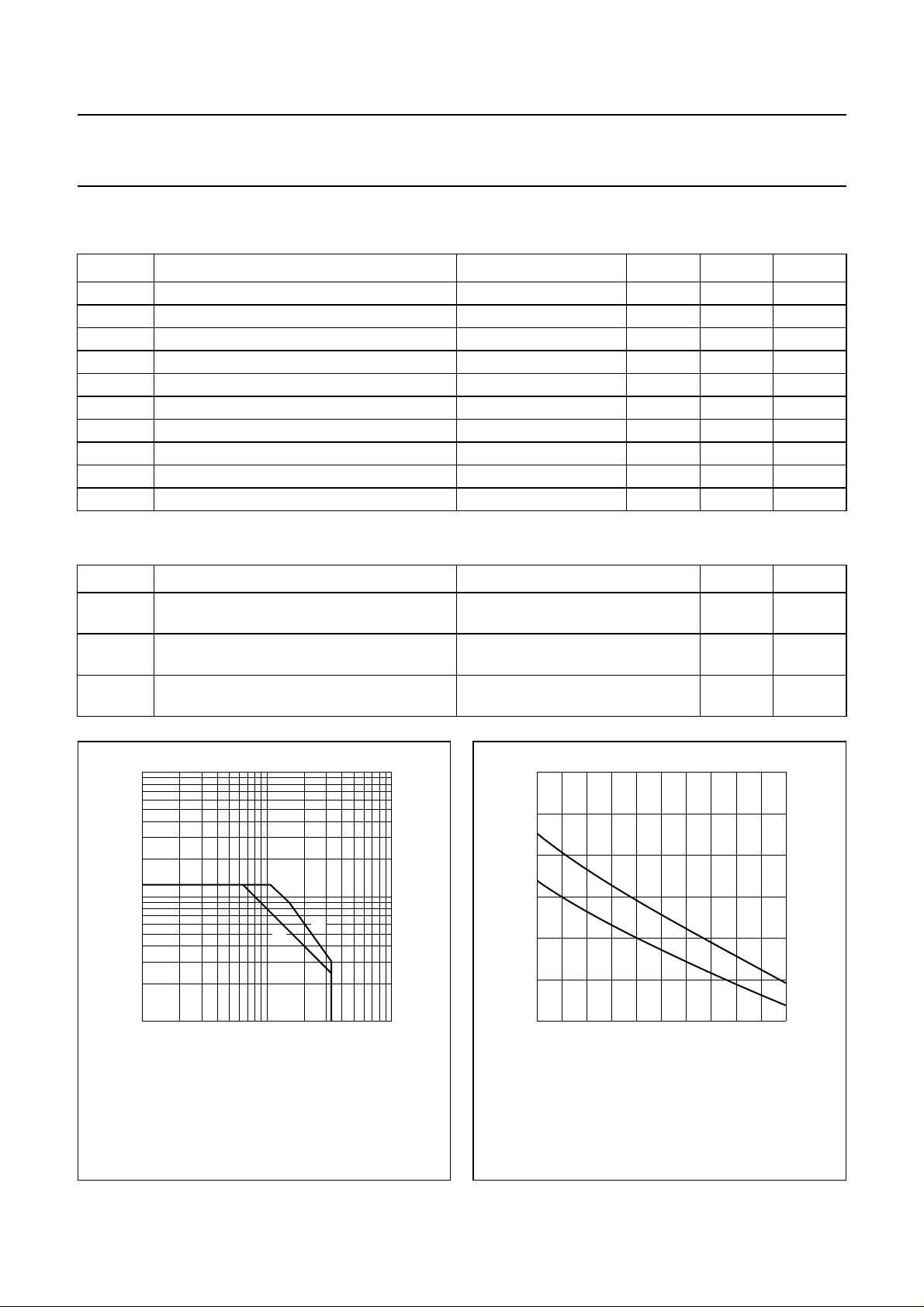
handbook, halfpage
(A)
thermal resistance from junction to mounting
base (DC dissipation)
thermal resistance from junction to mounting
base (RF dissipation)
thermal resistance from mounting base to
heatsink
2
10
I
C
10
1
11010
(1)
(2)
MGG132
(3)
V
(V)
CE
2
P
=80W; Tmb=82°C;
diss
Th=70°C
P
=80W; Tmb=82°C;
diss
Th=70°C
P
=80W; Tmb=82°C;
diss
Th=70°C
200
handbook, halfpage
P
tot
(W)
150
100
50
0 10050
1.43 K/W
1.17 K/W
0.2 K/W
MGG133
(2)
(1)
Th (°C)
(1) Tmb=25°C.
(2) Th=70°C.
(3) Second breakdown limit (independent of temperature).
Fig.2 DC SOAR.
1996 Oct 10 3
(1) Continuous DC (including RF class-A) operation.
(2) Continuous RF operation.
Fig.3 Power derating curves.
Page 4
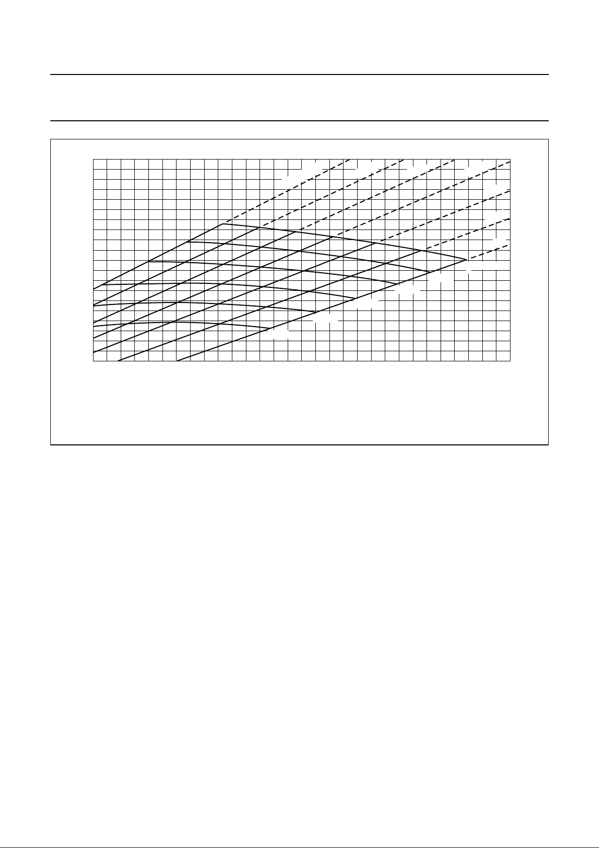
Philips Semiconductors Product specification
VHF linear power transistor BLV33F
2.0
handbook, full pagewidth
R
th j-h
(K/W)
1.8
1.6
1.4
1.2
1.0
0
R
= 0.2 K/W.
th mb-h
75 °C
= 120 °C
T
h
100 °C
100 °C
125 °C
10050
80 °C
150 °C
175 °C
P
tot
(W)
MGG144
60 °C
40 °C
20 °C
0 °C
Tj = 200 °C
Fig.4 Maximum thermal resistance from junction to heatsink as a function of power dissipation, with heatsink
and junction temperature as parameters.
150
Example
Nominal class-A operation (without RF signal): VCE= 25 V; IC= 3.2 A; Th=70°C.
Figure 4 shows:
R
= max. 1.63 K/W
th j-h
Tj= max. 200 °C.
Typical device:
R
= typ.1.53 K/W
th j-h
Tj= typ. 192 °C.
1996 Oct 10 4
Page 5
Philips Semiconductors Product specification
VHF linear power transistor BLV33F
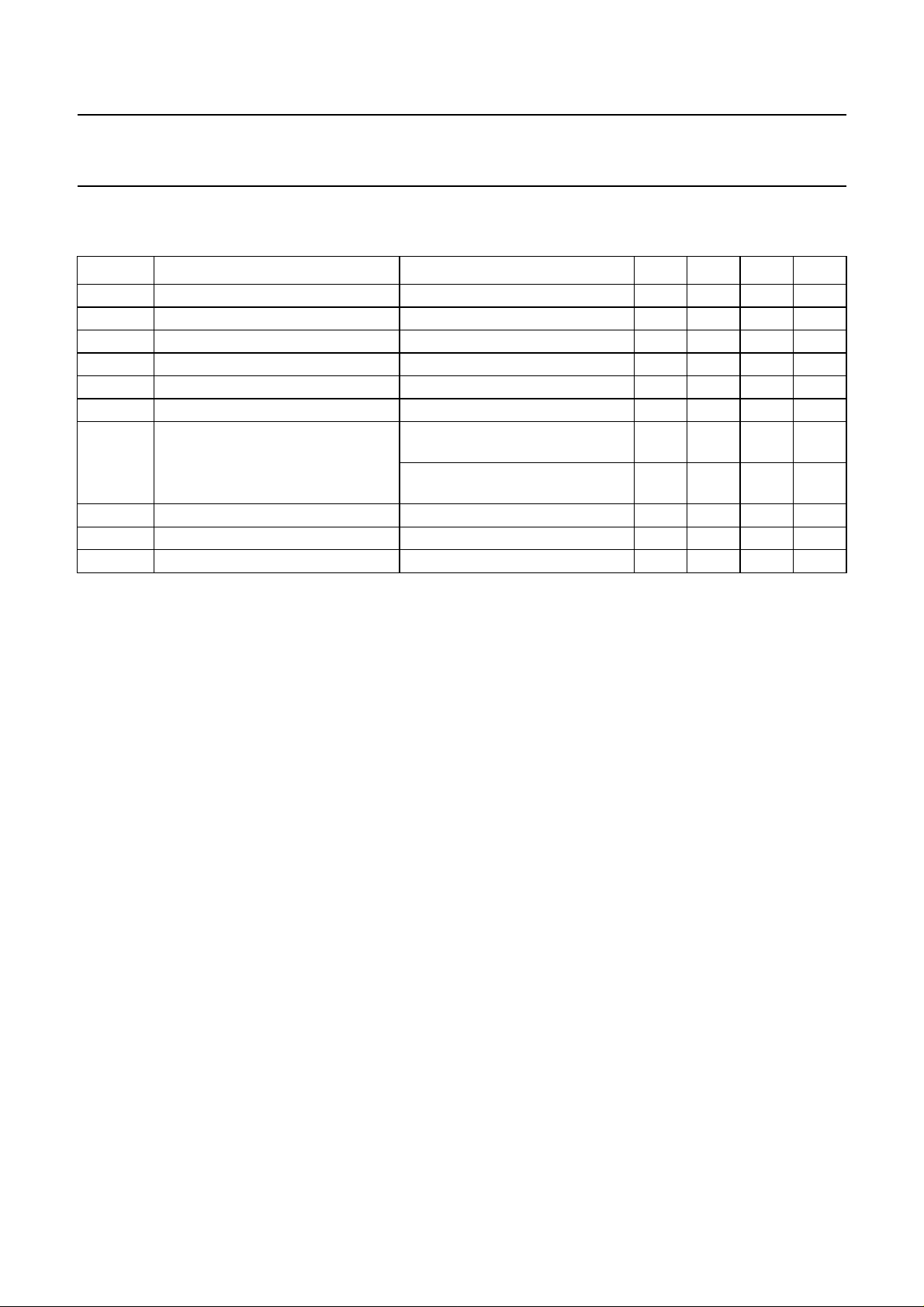
CHARACTERISTICS
T
=25°C; unless otherwise specified.
j
SYMBOL PARAMETER CONDITIONS MIN. TYP. MAX. UNIT
V
(BR)CES
V
(BR)CEO
V
(BR)EBO
I
CES
h
FE
V
CEsat
f
T
C
c
C
re
C
cf
collector-emitter breakdown voltage VBE= 0; IC=25mA 65 −−V
collector-emitter breakdown voltage open base; IC= 100 mA 33 −−V
emitter-base breakdown voltage open collector; IE=10mA 4 −−V
collector cut-off current VBE= 0; VCE=30V −−1mA
DC current gain VCE=25V; IC= 3 A; note 1 15 50 100
collector-emitter saturation voltage IC= 6 A; IB= 0.6 A; note 1 − 0.75 − V
transition frequency VCB=25V; IE=−3A;
− 680 − MHz
f = 100 MHz; note 2
V
=25V; IE=−6A;
CB
− 750 − MHz
f = 100 MHz; note 2
collector capacitance VCB=25V; IE=ie= 0; f = 1 MHz − 155 − pF
feedback capacitance IC= 50 mA; VCE=25V; f=1MHz − 88 − pF
collector-flange capacitance − 3 − pF
Notes
1. Measured under pulse conditions: t
≤ 300 µs; δ≤0.02.
p
2. Measured under pulse conditions: tp≤ 50 µs; δ≤0.01.
1996 Oct 10 5
Page 6
Philips Semiconductors Product specification
VHF linear power transistor BLV33F
75
handbook, halfpage
h
FE
50
25
0
05 15
Tj=25°C.
(1) VCE=25V.
(2) VCE=5V.
(1)
(2)
10
MGG130
IC (A)
Fig.5 DC current gain as a function of collector
current; typical values.
600
handbook, halfpage
C
c
(pF)
400
200
0
02040
IE=ie= 0; f = 1 MHz; Tj=25°C.
VCB (V)
Fig.6 Collector capacitance as a function of
collector-base voltage; typical values.
MGG129
1000
handbook, halfpage
f
T
(MHz)
800
600
400
200
0
−0 −5 −15
VCB= 25 V; f = 100 MHz; Tj=25°C.
−10
MGG131
IE (A)
Fig.7 Transition frequency as a function of emitter
current; typical values.
10
handbook, halfpage
I
C
(A)
1
−1
10
VCE=25V.
(1) Th=70°C.
(2) Th=25°C.
(1)
(2)
Fig.8 Collector current as a function of
base-emitter voltage; typical values.
MGG118
VBE (V)
20.5 1 1.5
1996 Oct 10 6
Page 7

Philips Semiconductors Product specification
VHF linear power transistor BLV33F
APPLICATION INFORMATION
RF performance in VHF class-A operation (linear power amplifier)
MODE OF
OPERATION
f
vision
(MHz)
V
(V)
CE
I
(A)
C
T
h
(°C)
d
im
(dB)
(1)
P
o sync
(W)
(1)
G
P
(dB)
70 −55 >13 >13.5
CW, class-A 224.25 25 3.2
70 −55 typ. 14.5 typ. 14.5
70 −52 typ. 22 typ. 14.5
25 −55 typ. 19 typ. 14.8
Note
1. Three-tone test method (vision carrier −8 dB, sound carrier −7 dB, sideband signal −16 dB), zero dB corresponds to
peak sync level.
handbook, full pagewidth
50 Ω
input
C1
C2
+V
BB
C3
L1
C4
C5
C6
L2
D.U.T.
C7
L3 L5
C8
C9
R1
L4
C11
C10
C12
+V
CC
C13
L6
C15
C14
50 Ω
output
MGG146
Fig.9 Class-A test circuit at f
1996 Oct 10 7
= 224.25 MHz.
vision
Page 8

Philips Semiconductors Product specification
VHF linear power transistor BLV33F
List of components used in test circuit (see Figs 9 and 10).
COMPONENT DESCRIPTION VALUE DIMENSIONS CATALOGUE No.
C1, C15 multilayer ceramic chip
capacitor; note 1
C2, C4, C12, C14 film dielectric trimmer 4 to 40 pF 2222 809 08002
C3 multilayer ceramic chip
capacitor; note 1
C5 multilayer ceramic chip
capacitor
C6, C10 multilayer ceramic chip
capacitor
C7, C8 multilayer ceramic chip
capacitor; note 1
C9 polyester capacitor 330 nF
C11 multilayer ceramic chip
capacitor; note 1
C13 solid tantalum capacitor 6.8 µF, 35 V
L1 2 turns of 1.6 mm enamelled
Cu wire
L2 microchoke 1 µH 4322 057 01080
L3 stripline; note 2 30 Ω 6mm×32.7 mm
L4 2 turns of closely wound
1 mm enamelled Cu wire
L5 stripline; note 2 30 Ω 6mm×24 mm
L6 2 turns of 1.6 mm enamelled
Cu wire
R1 carbon resistor 10 Ω
560 pF, 500 V
10 pF, 500 V
470 nF, 50 V 2222 856 48474
680 pF, 50 V 2222 852 13681
47 pF, 500 V placed 8 mm from
transistor edge
68 pF, 500 V
int. diameter 5 mm
length 5 mm
leads 2 × 3mm
int. diameter 5 mm
leads 2 × 10 mm
int. diameter 4 mm
length 4.5 mm
leads 2 × 3mm
Notes
1. American Technical Ceramics type 100B or capacitor of same quality.
2. The striplines are on a double Cu-clad printed-circuit board, with epoxy fibre-glass dielectric (ε
1996 Oct 10 8
= 4.5); thickness1⁄16".
r
Page 9

Philips Semiconductors Product specification
VHF linear power transistor BLV33F
handbook, full pagewidth
50
rivets
C2
rivets
C3
C5
115
rivets
rivets
+V
BB
C6
L2
C7
C10
+V
CC
C13
R1
C9
L4
C11
C14
50 Ω
input
Dimensions in mm.
The circuit and the components are on one side of the epoxy fibre-glass board, the other side is unetched copper to serve as earth. Earth connections
are made by hollow rivets. Additionally copper straps are used under the emitters and at the input and output to provide direct contact between the
copper on the component side and the ground-plane.
C1
L1
C4
L3
C8
L5
C12
L6
C15
MGG149
50 Ω
output
Fig.10 Component layout and printed-circuit board for 224.25 MHz class-A test circuit.
1996 Oct 10 9
Page 10

Philips Semiconductors Product specification
VHF linear power transistor BLV33F
P
o sync
MGG134
(W)
−44
handbook, halfpage
d
im
(dB)
G
−48
p
−52
−56
d
−60
−64
VCE= 25 V; IC= 3.2 A; f
(1) Th=25°C.
(2) Th=70°C.
im
10 20 30 40
(1)
(2)
(2) (1)
= 224.25 MHz.
vision
Fig.11 Intermodulation distortion and power gain
as a functions of output power.
30
handbook, halfpage
15
G
p
(dB)
14
13
12
11
d
cm
(%)
20
(2) (1)
10
0
02040
VCE= 25 V; IC= 3.2 A; f
(1) Th=25°C.
(2) Th=70°C.
= 224.25 MHz.
vision
P
o sync
MGG135
(W)
Fig.12 Cross-modulation distortion as a function of
output power.
Three-tone test method (vision carrier−8 dB, sound carrier −7 dB, sideband signal −16 dB), zero dB corresponds to peak
sync level (see Fig.11). Intermodulation distortion of input signal ≤−70 dB.
Two-tone test method (vision carrier 0 dB, sound carrier −7 dB), zero dB corresponds to peak sync level.
Cross-modulation distortion (dcm) is the voltage variation (%) of sound carrier when vision carrier is switched from
0dBto−20 dB (see Fig.12).
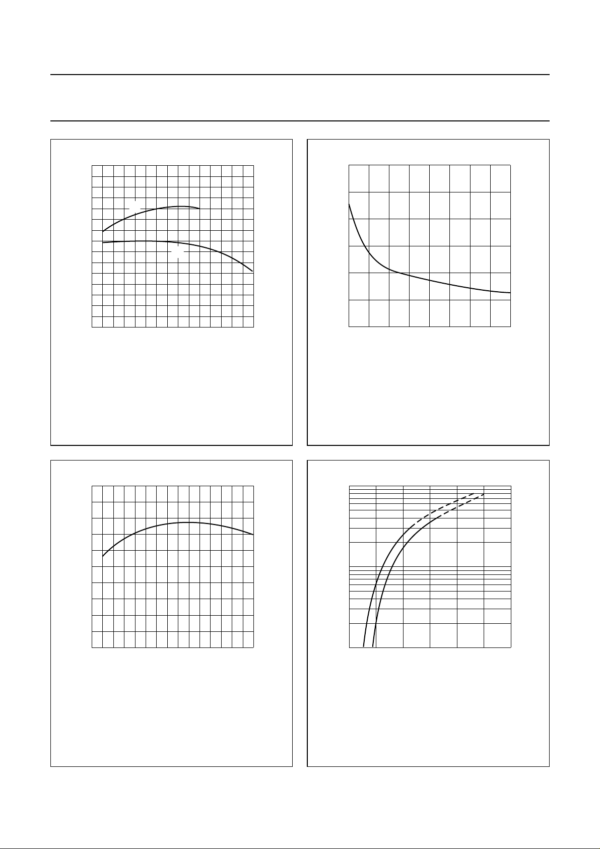
Ruggedness in class-A operation
The BLV33F is capable of withstanding a full load mismatch corresponding to VSWR = 50 : 1 through all phases up to
30 W (RMS) or 40 W (PEP) under the following conditions: V
R
th mb-h
= 0.2 K/W.
= 25 V; IC= 3.2 A; Th=70°C; f = 224.25 MHz;
CE
1996 Oct 10 10
Page 11

Philips Semiconductors Product specification
VHF linear power transistor BLV33F
handbook, halfpage
1
Z
i
(Ω)
0
−1
50 250
Class-A operation; VCE= 25 V; IC= 3.2 A; Th=70°C.
r
i
x
i
150
MGG136
f (MHz)
Fig.13 Input impedance as a function of frequency
(series components); typical values.
handbook, halfpage
6
Z
L
(Ω)
4
R
L
2
X
L
0
50 250150
Class-A operation; VCE= 25 V; IC= 3.2 A; Th=70°C.
MGG137
f (MHz)
Fig.14 Load impedance as a function of frequency
(series components); typical values.
30
handbook, halfpage
G
p
(dB)
20
10
0
50 250150
Class-A operation; VCE= 25 V; IC= 3.2 A; Th=70°C.
f (MHz)
Fig.15 Power gain as a function of frequency;
typical values.
MGG138
1996 Oct 10 11
Page 12

Philips Semiconductors Product specification
VHF linear power transistor BLV33F
RF performance in VHF class-AB operation (C.W.).
MODE OF
OPERATIONf(MHz)
CW, class-AB 224.25 28 0.2 70
V
(V)
CE
IC, I
C(ZS)
(A)
T
(°C)
h
P
L
(W)
I
(A)
C
η
C
(%)
40 typ. 2.75 typ. 52 typ. 11.5
85 typ. 4.25 typ. 71 typ. 10.5
Note
1. Gain compression point of 1 dB is at typical 85 W (minimum 75 W). Using a 3rd-order amplitude transfer
characteristic, 1 dB compression corresponds with 30 % sync input / 25 % sync output compression in television
service (negative modulation, C.C.I.R. system).
handbook, full pagewidth
50 Ω
C1
C2
C3
+V
BB
C4
L1
C5
C6
C7
L2
D.U.T.
C8
L3 L5
C9
C10
R1
C11
C12
+V
CC
C15
L4
C13
C14
C16
L6
C18
50 Ω
C17
MGG147
G
(dB)
P
(1)
Fig.16 Class-AB test circuit at f
1996 Oct 10 12
= 224.25 MHz.
vision
Page 13

Philips Semiconductors Product specification
VHF linear power transistor BLV33F
List of components used in test circuit (see Figs 16 and 17).
COMPONENT DESCRIPTION VALUE DIMENSIONS CATALOGUE No.
C1, C18 multilayer ceramic chip
capacitor; note 1
C2 multilayer ceramic chip
capacitor; note 1
C3 film dielectric trimmer 2 to 18 pF 2222 809 09003
C4 multilayer ceramic chip
capacitor; note 1
C5, C14 film dielectric trimmer 4 to 40 pF 2222 809 08002
C6, C10 multilayer ceramic chip
capacitor
C7, C15 multilayer ceramic chip
capacitor
C8, C9 multilayer ceramic chip
capacitor; note 1
C11, C12 multilayer ceramic chip
capacitor; note 1
C13 multilayer ceramic chip
capacitor; note 1
C16 multilayer ceramic chip
capacitor; note 1
C17 film dielectric trimmer 1.4 to 5.5 pF 2222 809 09001
L1 2 turns of 1.6 mm enamelled
Cu wire
L2 3 turns of 1 mm closely
wound enamelled Cu wire
L3 stripline; note 2 30 Ω 6mm×47.8 mm
L4 2 turns of 1 mm closely
wound enamelled Cu wire
L5 stripline; note 2 30 Ω 6mm×42.9 mm
L6 2 turns of 1.6 mm enamelled
Cu wire
R1 carbon resistor 10 Ω
620 pF, 100 V
27 pF, 500 V
30 pF, 500 V
470 nF, 50 V 2222 856 48474
680 pF, 50 V 2222 852 13681
68 pF, 500 V placed 6.4 mm from
transistor edge
43 pF, 500 V placed 10 mm from
transistor edge
39 pF, 500 V
3.3 pF, 500 V
int. diameter 4.5 mm
length 4 mm
leads 2 × 4mm
int. diameter 5 mm
leads 2 × 7mm
int. diameter 5 mm
leads 2 × 8mm
int. diameter 4 mm
length 4 mm
leads 2 × 3mm
Notes
1. American Technical Ceramics type 100B or capacitor of same quality.
2. The striplines are on a double Cu-clad printed-circuit board, with epoxy fibre-glass dielectric (ε
1996 Oct 10 13
= 4.5); thickness1⁄16".
r
Page 14

Philips Semiconductors Product specification
VHF linear power transistor BLV33F
handbook, full pagewidth
57
50 Ω
input
C1
C2
rivets
C3
rivets
150
rivets
rivets
+V
BB
C6
C4
L1
L3
C7
L2
C8
C9
C15
L4
+V
CC
C10
C11
C12
C17
R1
C13
L5
L6
C18
C16
50 Ω
output
C5
C14
MGG151
Dimensions in mm.
The circuit and the components are on one side of the epoxy fibre-glass board, the other side is unetched copper to serve as earth. Earth connections
are made by hollow rivets. Additionally copper straps are used under the emitters and at the input and output to provide direct contact between the
copper on the component side and the ground-plane.
Fig.17 Component layout and printed-circuit board for 224.25 MHz class-AB test circuit.
1996 Oct 10 14
Page 15

Philips Semiconductors Product specification
VHF linear power transistor BLV33F
100
handbook, halfpage
P
L
(W)
80
60
40
20
0
024 8
VCE= 28 V; I
= 0.2 A; Th=70°C; f
C(ZS)
vision
MGG139
6
PS (W)
= 224.25 MHz.
Fig.18 Load power as a function of source power;
typical values.
Ruggedness in class-AB operation
15
handbook, halfpage
G
p
(dB)
10
5
0 100
VCE= 28 V; I
= 0.2 A; Th=70°C; f
C(ZS)
η
c
G
p
50
vision
MGG140
PL (W)
= 224.25 MHz.
Fig.19 Power gain and efficiency as functions of
load power; typical values.
75
50
25
η
(%)
c
The BLV33F is capable of withstanding a full load mismatch corresponding to VSWR ≤2 through all phases) up to
60 W (RMS) and 85 W (PEP) under the following conditions:VCE= 28 V; Th=70°C; f = 224.25 MHz; R
th mb-h
= 0.2 K/W.
1996 Oct 10 15
Page 16

Philips Semiconductors Product specification
VHF linear power transistor BLV33F
handbook, halfpage
1
Z
i
(Ω)
0
−1
50 250
Class-AB operation; VCE= 28 V; PL= 80 W (PEP); Th=70°C.
r
i
x
i
150
MGG141
f (MHz)
Fig.20 Input impedance as a function of frequency
(series components); typical values.
handbook, halfpage
4
Z
L
(Ω)
2
0
50 250150
Class-AB operation; VCE= 28 V; PL= 80 W (PEP); Th=70°C.
R
L
X
L
MGG142
f (MHz)
Fig.21 Load impedance as a function of frequency
(series components); typical values.
20
handbook, halfpage
G
p
(dB)
10
0
50 250
Class-AB operation; VCE= 28 V; PL= 80 W (PEP); Th=70°C.
150
MGG143
f (MHz)
Fig.22 Power gain as a function of frequency;
typical values.
1996 Oct 10 16
Page 17

Philips Semiconductors Product specification
VHF linear power transistor BLV33F
PACKAGE OUTLINE
handbook, full pagewidth
12.96
6.48
22 max
6.35
1
5.5
3
5.0
56
12.2
2.5
3.35
3.04
4
min
5.7
2
5.3
3.8
4
min
5.7
5.3
(2x)
4.50
4.05
7.5
max
25.2
max
18.42
0.14
ceramic
metal
MBC877
BeO
13
max
Dimensions in mm.
Torque on screw: min. 0.6 Nm; max. 0.75 Nm.
Recommended screw: cheese-head 4-40 UNC/2A.
Heatsink compound must be applied sparingly and evenly distributed.
Fig.23 SOT119A.
1996 Oct 10 17
Page 18

Philips Semiconductors Product specification
VHF linear power transistor BLV33F
DEFINITIONS
Data Sheet Status
Objective specification This data sheet contains target or goal specifications for product development.
Preliminary specification This data sheet contains preliminary data; supplementary data may be published later.
Product specification This data sheet contains final product specifications.
Limiting values
Limiting values given are in accordance with the Absolute Maximum Rating System (IEC 134). Stress above one or
more of the limiting values may cause permanent damage to the device. These are stress ratings only and operation
of the device at these or at any other conditions above those given in the Characteristics sections of the specification
is not implied. Exposure to limiting values for extended periods may affect device reliability.
Application information
Where application information is given, it is advisory and does not form part of the specification.
LIFE SUPPORT APPLICATIONS
These products are not designed for use in life support appliances, devices, or systems where malfunction of these
products can reasonably be expected to result in personal injury. Philips customers using or selling these products for
use in such applications do so at their own risk and agree to fully indemnify Philips for any damages resulting from such
improper use or sale.
1996 Oct 10 18
Page 19

Philips Semiconductors Product specification
VHF linear power transistor BLV33F
NOTES
1996 Oct 10 19
Page 20

Philips Semiconductors – a worldwide company
Argentina: see South America
Australia: 34 Waterloo Road, NORTH RYDE, NSW 2113,
Tel. +61 2 9805 4455, Fax. +61 2 9805 4466
Austria: Computerstr. 6, A-1101 WIEN, P.O. Box 213,
Tel. +43 1 60 101, Fax. +43 1 60 101 1210
Belarus: Hotel Minsk Business Center, Bld. 3, r. 1211, Volodarski Str. 6,
220050 MINSK, Tel. +375 172 200 733, Fax. +375 172 200 773
Belgium: see The Netherlands
Brazil: see South America
Bulgaria: Philips Bualgaria Ltd., Energoproject, 15th floor,
51 James Bourchier Blvd., 1407 SOFIA,
Tel. +359 2 689 211, Fax. +359 2 689 102
Canada: PHILIPS SEMICONDUCTORS/COMPONENTS,
Tel. +1 800 234 7381
China/Hong Kong: 501 Hong Kong Industrial Technology Centre,
72 Tat Chee Avenue, Kowloon Tong, HONG KONG,
Tel. +852 2319 7888, Fax. +852 2319 7700
Colombia: see South America
Czech Republic: see Austria
Denmark: Prags Boulevard 80, PB 1919, DK-2300 COPENHAGEN S,
Tel. +45 32 88 2636, Fax. +45 31 57 1949
Finland: Sinikalliontie 3, FIN-02630 ESPOO,
Tel. +358 9 615800, Fax. +358 9 61580/xxx
France: 4 Rue du Port-aux-Vins, BP317, 92156 SURESNES Cedex,
Tel. +33 1 40 99 6161, Fax. +33 1 40 99 6427
Germany: Hammerbrookstraße 69, D-20097 HAMBURG,
Tel. +49 40 23 53 60, Fax. +49 40 23 536 300
Greece: No. 15, 25th March Street, GR 17778 TAVROS/ATHENS,
Tel. +30 1 4894 339/239, Fax. +30 1 4814 240
Hungary: see Austria
India: Philips INDIA Ltd, Shivsagar Estate, A Block, Dr. Annie Besant Rd.
Worli, MUMBAI 400 018, Tel. +91 22 4938 541, Fax. +91 22 4938 722
Indonesia: see Singapore
Ireland: Newstead, Clonskeagh, DUBLIN 14,
Tel. +353 1 7640 000, Fax. +353 1 7640 200
Israel: RAPAC Electronics, 7 Kehilat Saloniki St, TEL AVIV 61180,
Tel. +972 3 645 0444, Fax. +972 3 649 1007
Italy: PHILIPS SEMICONDUCTORS, Piazza IV Novembre 3,
20124 MILANO, Tel. +39 2 6752 2531, Fax. +39 2 6752 2557
Japan: Philips Bldg 13-37, Kohnan 2-chome, Minato-ku, TOKYO 108,
Tel. +81 3 3740 5130, Fax. +81 3 3740 5077
Korea: Philips House, 260-199 Itaewon-dong, Yongsan-ku, SEOUL,
Tel. +82 2 709 1412, Fax. +82 2 709 1415
Malaysia: No. 76 Jalan Universiti, 46200 PETALING JAYA, SELANGOR,
Tel. +60 3 750 5214, Fax. +60 3 757 4880
Mexico: 5900 Gateway East, Suite 200, EL PASO, TEXAS 79905,
Tel. +9-5 800 234 7381
Middle East: see Italy
Netherlands: Postbus 90050, 5600 PB EINDHOVEN, Bldg. VB,
Tel. +31 40 27 82785, Fax. +31 40 27 88399
New Zealand: 2 Wagener Place, C.P.O. Box 1041, AUCKLAND,
Tel. +64 9 849 4160, Fax. +64 9 849 7811
Norway: Box 1, Manglerud 0612, OSLO,
Tel. +47 22 74 8000, Fax. +47 22 74 8341
Philippines: Philips Semiconductors Philippines Inc.,
106 Valero St. Salcedo Village, P.O. Box 2108 MCC, MAKATI,
Metro MANILA, Tel. +63 2 816 6380, Fax. +63 2 817 3474
Poland: Ul. Lukiska 10, PL 04-123 WARSZAWA,
Tel. +48 22 612 2831, Fax. +48 22 612 2327
Portugal: see Spain
Romania: see Italy
Russia: Philips Russia, Ul. Usatcheva 35A, 119048 MOSCOW,
Tel. +7 095 247 9145, Fax. +7 095 247 9144
Singapore: Lorong 1, Toa Payoh, SINGAPORE 1231,
Tel. +65 350 2538, Fax. +65 251 6500
Slovakia: see Austria
Slovenia: see Italy
South Africa: S.A. PHILIPS Pty Ltd., 195-215 Main Road Martindale,
2092 JOHANNESBURG, P.O. Box 7430 Johannesburg 2000,
Tel. +27 11 470 5911, Fax. +27 11 470 5494
South America: Rua do Rocio 220, 5th floor, Suite 51,
04552-903 São Paulo, SÃO PAULO - SP, Brazil,
Tel. +55 11 821 2333, Fax. +55 11 829 1849
Spain: Balmes 22, 08007 BARCELONA,
Tel. +34 3 301 6312, Fax. +34 3 301 4107
Sweden: Kottbygatan 7, Akalla, S-16485 STOCKHOLM,
Tel. +46 8 632 2000, Fax. +46 8 632 2745
Switzerland: Allmendstrasse 140, CH-8027 ZÜRICH,
Tel. +41 1 488 2686, Fax. +41 1 481 7730
Taiwan: PHILIPS TAIWAN Ltd., 23-30F, 66,
Chung Hsiao West Road, Sec. 1, P.O. Box 22978,
TAIPEI 100, Tel. +886 2 382 4443, Fax. +886 2 382 4444
Thailand: PHILIPS ELECTRONICS (THAILAND) Ltd.,
209/2 Sanpavuth-Bangna Road Prakanong, BANGKOK 10260,
Tel. +66 2 745 4090, Fax. +66 2 398 0793
Turkey: Talatpasa Cad. No. 5, 80640 GÜLTEPE/ISTANBUL,
Tel. +90 212 279 2770, Fax. +90 212 282 6707
Ukraine: PHILIPS UKRAINE, 4 Patrice Lumumba str., Building B, Floor 7,
252042 KIEV, Tel. +380 44 264 2776, Fax. +380 44 268 0461
United Kingdom: Philips Semiconductors Ltd., 276 Bath Road, Hayes,
MIDDLESEX UB3 5BX, Tel. +44 181 730 5000, Fax. +44 181 754 8421
United States: 811 East Arques Avenue, SUNNYVALE, CA 94088-3409,
Tel. +1 800 234 7381
Uruguay: see South America
Vietnam: see Singapore
Yugoslavia: PHILIPS, Trg N. Pasica 5/v, 11000 BEOGRAD,
Tel. +381 11 625 344, Fax.+381 11 635 777
For all other countries apply to: Philips Semiconductors, Marketing & Sales Communications,
Building BE-p, P.O. Box 218, 5600 MD EINDHOVEN, The Netherlands, Fax. +31 40 27 24825
© Philips Electronics N.V. 1996 SCA52
All rights are reserved. Reproduction in whole or in part is prohibited without the prior written consent of the copyright owner.
The information presented in this document does not form part of any quotation or contract, is believed to be accurate and reliable and may be changed
without notice. No liability will be accepted by the publisher for any consequence of its use. Publication thereof does not convey nor imply any license
under patent- or other industrial or intellectual property rights.
Internet: http://www.semiconductors.philips.com
Printed in The Netherlands 127041/1200/01/pp20 Date of release: 1996 Oct 10 Document order number: 9397 750 01036
 Loading...