

Page 1

DISCRETE SEMICONDUCTORS
DATA SH EET
BLV25
VHF power transistor
Product specification
August 1986
Page 2

Philips Semiconductors Product specification
VHF power transistor BLV25
DESCRIPTION
N-P-N silicon planar epitaxial
transistor primarily for use in
v.h.f.-f.m. broadcast transmitters.
FEATURES
• internally matched input for
wideband operation and high
power gain;
• multi-base structure and diffused
emitter ballasting resistors for an
optimum temperature profile;
• gold-metallization ensures
excellent reliability.
The transistor has a1⁄2in 6-lead
flange envelope with a ceramic cap.
All leads are isolated from the flange.
QUICK REFERENCE DATA
R.F. performance up to T
MODE OPERATION
=25°C in an unneutralized common-emitter class-B circuit.
h
V
CE
V
f
MHz
P
W
L
P
S
W
G
dB
p
narrow band; c.w. 28 108 175 < 17,5 > 10,0 > 65
PIN CONFIGURATION
PINNING
PIN DESCRIPTION
1 emitter
handbook, halfpage
1
2
2 emitter
3 base
3
4
4 collector
5 emitter
6 emitter
65
η
%
MSB006
Fig.1 Simplified outline, SOT119A.
PRODUCT SAFETY This device incorporates beryllium oxide, the dust of which is toxic. The device is entirely
safe provided that the BeO disc is not damaged.
August 1986 2
Page 3
Philips Semiconductors Product specification
VHF power transistor BLV25
RATINGS
Limiting values in accordance with the Absolute Maximum System (IEC 134)
Collector-emitter voltage
(peak value); V
open base V
Emitter-base voltage (open collector) V
Collector current
d.c. or average I
(peak value); f > 1 MHz I
Total power dissipation at T
R.F. power dissipation (f > 1 MHz); T
R.F. power dissipation (f > 1 MHz); T
Storage temperature T
Operating junction temperature T
=0 V
BE
=25°CP
mb
=25°CP
mb
=70°CP
h
CESM
CEO
EBO
; I
C
C(AV)
CM
tot (d.c.)
tot (r.f.)
tot (r.f.)
stg
j
max. 65 V
max. 33 V
max. 4 V
max. 17, 5 A
max. 35 A
max. 220 W
max. 270 W
max. 146 W
−65 to +150 °C
max. 200 °C
2
10
handbook, halfpage
I
C
(A)
10
1
11010
(1) Second breakdown limit.
Tmb = 25 °C
Th = 70 °C
Fig.2 D.C. SOAR.
(1)
VCE (V)
MGP294
2
300
handbook, halfpage
P
tot
(W)
200
100
0
0 100
I Continuous d.c. operation
II Continuous r.f. operation (f > 1 MHz)
III Short-time operation during mismatch; (f > 1 MHz).
ΙΙΙ
ΙΙ
Ι
50
Th (°C)
Fig.3 Power derating curves vs. temperature.
MGP295
THERMAL RESISTANCE
(dissipation = 150 W; T
=72°C, i.e. Th=42°C)
mb
From junction to mounting base (d.c. dissipation) R
From junction to mounting base (r.f. dissipation) R
From mounting base to heatsink R
August 1986 3
th j-mb(dc)
th j-mb(rf)
th mb-h
max 0,85 K/W
max 0,60 K/W
max 0,2 K/W
Page 4

Philips Semiconductors Product specification
VHF power transistor BLV25
CHARACTERISTICS
T
=25°C
j
Collector-emitter breakdown voltage
V
=0;IC=50mA V
BE
open base; I
= 200 mA V
C
Emitter-base breakdown voltage
open collector; I
=20mA V
E
Collector cut-off current
VBE=0;VCE= 33 V I
Second breakdown energy; L = 25 mH; f = 50 Hz
open base E
R
=10Ω E
BE
D.C. current gain
(1)
IC= 8,5 A; VCE=25V h
Collector-emitter saturation voltage
(1)
IC= 20 A; IB= 4,0 A V
Transition frequency at f = 100 MHz
(2)
−IE= 8,5 A; VCB=25V f
−I
= 20 A; VCB=25V f
E
Collector capacitance at f = 1 MHz
I
= 0; VCB=25V C
E=Ie
Feedback capacitance at f=1MHz
IC= 100 mA; VCE=25V C
Collector-flange capacitance C
(BR)CES
(BR)CEO
(BR)EBO
CES
SBO
SBR
FE
CEsat
T
T
c
re
cf
> 65 V
> 33 V
> 4V
< 25 mA
> 20 mJ
> 20 mJ
typ. 50
15 to 100
typ. 1,6 V
typ. 600 MHz
typ. 600 MHz
typ. 275 pF
typ. 155 pF
typ. 3 pF
Notes
1. Measured under pulse conditions: t
≤ 300 µs; δ≤0,02.
p
2. Measured under pulse conditions: tp≤ 50 µs; δ≤0,01.
August 1986 4
Page 5

Philips Semiconductors Product specification
VHF power transistor BLV25
80
handbook, halfpage
h
FE
40
0
0
typ
10
IC (A)
Fig.4 VCE= 25 V; Tj=25°C.
MGP296
800
handbook, halfpage
f
T
(MHz)
400
20
0
010 30
typ
20
MGP297
−IE (A)
Fig.5 VCB= 25 V; f = 100 MHz; Tj=25°C.
600
handbook, halfpage
C
c
(pF)
300
0
0102030
typ
MGP298
VCB (V)
Fig.6 IE=Ie= 0; f = 1 MHz; Tj=25°C.
August 1986 5
Page 6

Philips Semiconductors Product specification
VHF power transistor BLV25
APPLICATION INFORMATION
R.F. performance in narrow band c.w. operation (common-emitter class-B circuit) T
=25°C
h
f
MHz
V
CE
V
P
W
L
P
S
W
G
dB
p
I
C
A
108 28 175 < 17,5 > 10,0 < 9,6 > 65
typ. 13,9 typ. 11,0 typ. 8,9 typ. 70
handbook, full pagewidth
50 Ω
C1
C2
C3
C4
L1
L3
R1
C5
T.U.T.
L2
C6
C7
L4
L6
L5
C8 C10 C11 C14
L7
C9
C12
C13
C15
50 Ω
C16
L8
+V
L9
MGP299
Fig.7 Class-B test circuit at f = 108 MHz.
List of components
C1 = C3 = 7 to 100 pF film dielectric trimmer (cat. no. 2222 809 07015)
C2 = C4 = C5 = C6 = C7 = 100 pF (500 V) multilayer ceramic chip capacitor (ATC
(1)
); except for C2 these capacitors
are placed 7 mm from transistor edge
C8 = C10 = 470 pF multilayer ceramic chip capacitor (cat. no. 2222 856 13471)
C9 = C15 = 40 pF, parallel connection of 4 x 10 pF lead feed-through capacitors (cat. no. 2222 702 05109)
C11 = 100 nF multilayer ceramic chip capacitor (cat. no. 2222 852 59104)
C12 = C16 = 7 to 47 pF precision tuning capacitor (cat. no. 2222 805 00174)
C13 = 19 pF, parallel connection of 4 x 4,7 pF lead feed-through capacitors (cat. no. 2222 702 04478)
C14 = 6,8 µF/63 V electrolytic capacitor
η
%
CC
L1 = Cu strip (10 mm × 4 mm × 0,5 mm)
L2 = strip on printed-circuit board
L3 = 7 turns closely wound enamelled Cu wire (0,3 mm); int. dia. 3,0 mm; leads 2 × 6 mm
L4 = L8 = L9 = Ferroxcube wide-band h.f. choke, grade 3B (cat. no. 4312 020 36640)
L5 = 3 turns enamelled Cu wire (1,6 mm); int. dia. 8 mm; length 9 mm; leads 2 × 5 mm
L6 = Cu strip (27 mm × 9 mm × 0,5 mm)
L7 = 2 turns enamelled Cu wire (1,6 mm); int. dia. 8 mm; length 9 mm; leads 2 × 10 mm
L2 is strip on a double Cu-clad printed-circuit board with epoxy fibre-glass dielectric, thickness 1/16 in.
R1 = 10 Ω carbon resistor
Note
1. ATC means American Technical Ceramics.
August 1986 6
Page 7

Philips Semiconductors Product specification
VHF power transistor BLV25
270
80
C8
L4
C2
The circuit and the components are on one side of the epoxy fibre-glass board, the other side is unetched copper to serve as a
ground-plane. Earth connections are made by means of fixing screws. Additionally copper straps are used under the emitters and
at the input and output to provide direct contact between the copper on the component side and the ground-plane.
L3
L1
L2
C6, C7
C3C1
R1
C4, C5
7 mm
C10
C11
+V
CC
L7
L5
L8, L9
L6
C9
strip
C13
strip
stop
strip
C12
C15
stop
C16
Fig.8 Component layout and printed-circuit board for 108 MHz class-B test circuit.
strip
MGP300
August 1986 7
Page 8

Philips Semiconductors Product specification
VHF power transistor BLV25
200
handbook, halfpage
P
L
(W)
100
0
11010
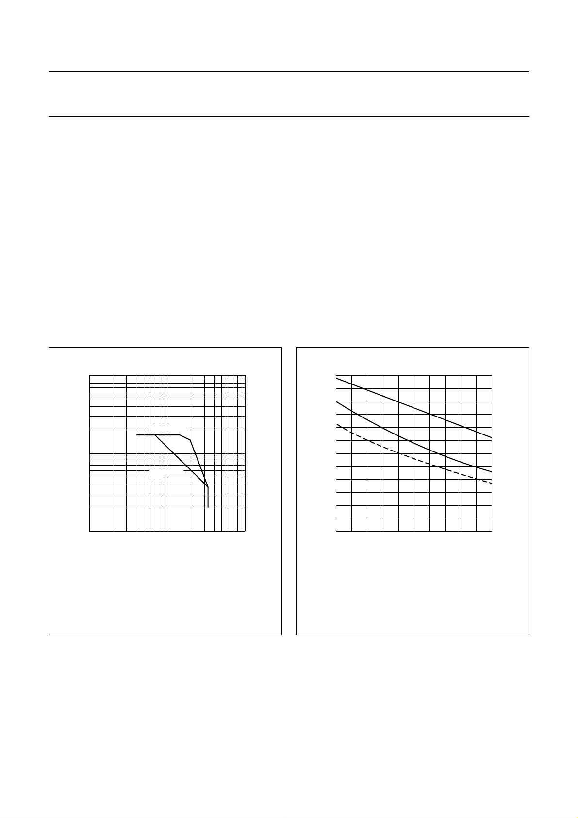
——— f > 1 MHz (continuous);
− − − − short time operation during mismatch (f > 1 MHz).
Th =
25 °C
50 °C
70 °C
25 °C
50 °C
70 °C
VSWR
Fig.9 R.F. SOAR.
MGP301
2
250
handbook, halfpage
P
L
(W)
200
150
100
50
0
0102030
Test circuit tuned for each power level; typical values;
= 28 V; f = 108 MHz; Th=25°C; class-B operation.
V
CE
MGP302
PS (W)
Fig.10 Load power as a function of source power.
16
handbook, halfpage
G
p
(dB)
12
8
4
0
0 100 200 300
Test circuit tuned for each power level; typical values;
= 28 V; f = 108 MHz; Th=25°C; class-B operation.
V
CE
η
G
p
MGP303
PL (W)
Fig.11 Power gain and efficiency as a function of
source power.
80
60
40
20
0
(%)
handbook, halfpage
η
1
ri, x
i
(Ω)
r
0.5
0
−0.5
−1
20
Typical values; VCE= 28 V; PL= 175 W;
=25°C; class-B operation.
T
h
i
x
i
70
f (MHz)
MGP304
120
Fig.12 Input impedance (series components).
August 1986 8
Page 9

Philips Semiconductors Product specification
VHF power transistor BLV25
handbook, halfpage
3
RL, X
L
(Ω)
2
1
0
20
Typical values; VCE= 28 V; PL= 175 W;
=25°C; class-B operation.
T
h
R
X
70
L
L
f (MHz)
Fig.13 Load impedance (series components).
MGP305
120
20
handbook, halfpage
G
p
(dB)
10
0
20 120
Typical values; VCE= 28 V; PL= 175 W;
=25°C; class-B operation.
T
h
70
f (MHz)
Fig.14 Power gain as a function of frequency.
MGP306
OPERATING NOTE for Figs 12, 13 and 14:
Below 50 MHz a base-emitter resistor of 4,7 Ω is
recommended to avoid oscillation. This resistor must be
effective for r.f. only.
August 1986 9
Page 10

Philips Semiconductors Product specification
VHF power transistor BLV25
PACKAGE OUTLINE
Flanged ceramic package; 2 mounting holes; 6 leads SOT119A
A
F
q
U
1
H
1
b
2
2
H
U
2
A
1
4
3
b
1
b
e
0 5 10 mm
6
5
C
scale
w
w
2
3
B
p
M
M
C
c
D
1DU3
w
M
AB
1
Q
DIMENSIONS (millimetre dimensions are derived from the original inch dimensions)
A
UNIT
7.39
mm
6.32
0.291
inches
0.249
OUTLINE
VERSION
SOT119A 97-06-28
5.59
5.33
0.220
0.210
b
1
5.34
5.08
0.210
0.200
c
0.18
0.07
0.007
0.003
Db
12.86
12.59
0.505
0.496
FH
eU
D
1
12.83
12.57
0.505
0.255
0.495
REFERENCES
6.48
2.54
2.28
0.100
0.090
22.10
21.08
0.870
0.830
b
2
4.07
3.81
0.160
0.150
IEC JEDEC EIAJ
H
18.55
18.28
0.730
0.720
qw
p
3.31
2.97
0.130
0.117
Q
4.58
3.98
0.180
0.157
1
U
1
6.48
25.23
6.07
23.95
0.255
0.993
0.239
0.943
EUROPEAN
PROJECTION
2
12.76
12.06
0.502
0.475
August 1986 10
U
3
w
1
2
0.5118.42
0.020.725 0.010.04
ISSUE DATE
w
3
0.261.02
Page 11

Philips Semiconductors Product specification
VHF power transistor BLV25
DEFINITIONS
Data Sheet Status
Objective specification This data sheet contains target or goal specifications for product development.
Preliminary specification This data sheet contains preliminary data; supplementary data may be published later.
Product specification This data sheet contains final product specifications.
Limiting values
Limiting values given are in accordance with the Absolute Maximum Rating System (IEC 134). Stress above one or
more of the limiting values may cause permanent damage to the device. These are stress ratings only and operation
of the device at these or at any other conditions above those given in the Characteristics sections of the specification
is not implied. Exposure to limiting values for extended periods may affect device reliability.
Application information
Where application information is given, it is advisory and does not form part of the specification.
LIFE SUPPORT APPLICATIONS
These products are not designed for use in life support appliances, devices, or systems where malfunction of these
products can reasonably be expected to result in personal injury. Philips customers using or selling these products for
use in such applications do so at their own risk and agree to fully indemnify Philips for any damages resulting from such
improper use or sale.
August 1986 11
 Loading...