

Page 1

DISCRETE SEMICONDUCTORS
DATA SH EET
BLV193
UHF power transistor
Product specification
March 1993
Page 2
Philips Semiconductors Product specification
UHF power transistor BLV193
FEATURES
• Emitter ballasting resistors for an
optimum temperature profile
• Gold metallization ensures
excellent reliability.
DESCRIPTION
NPN silicon planar epitaxial transistor
intended for common emitter class-A
and class-AB operation in the
900 MHz communications band.
The transistor has a SOT171 flange
envelope with a ceramic cap. All
leads are isolated from the mounting
base.
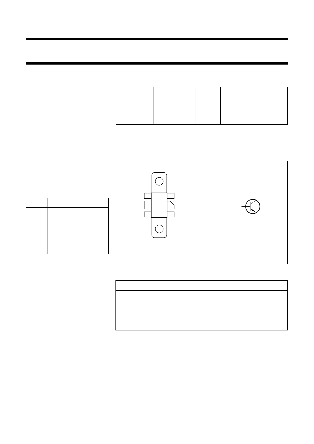
PINNING - SOT171
PIN DESCRIPTION
1 emitter
2 emitter
3 base
4 collector
5 emitter
6 emitter
QUICK REFERENCE DATA
RF performance at T
MODE OF
OPERATIONf(MHz)
= 25 °C in a common emitter test circuit.
h
V
(V)
CE
P
(W)
L
G
p
(dB)
η
(%)
C
d
(dB)
(note 1)
c.w. class-AB 900 12.5 12 ≥ 6.5 ≥ 50 −
c.w. class-A 900 12 6 (PEP) typ. 11 − typ. −30
Note
1. 2-tone measurement, f
= 900 MHz, fq= 901 MHz.
p
PIN CONFIGURATION
alfpage
1
3
5
Top view
2
4
6
MBA931 - 1
handbook, halfpage
b
MBB012
c
e
Fig.1 Simplified outline and symbol.
im
Product and environmental safety - toxic materials
This product contains beryllium oxide. The product is entirely safe provided
that the BeO disc is not damaged. All persons who handle, use or dispose of
this product should be aware of its nature and of the necessary safety
precautions. After use, dispose of as chemical or special waste according to
the regulations applying at the location of the user. It must never be thrown
out with the general or domestic waste.
March 1993 2
WARNING
Page 3

Philips Semiconductors Product specification
UHF power transistor BLV193
LIMITING VALUES
In accordance with the Absolute Maximum System (IEC 134).
SYMBOL PARAMETER CONDITIONS MIN. MAX. UNIT
V
CBO
V
CEO
V
EBO
I
C
P
tot
T
stg
T
j
collector-base voltage open emitter − 36 V
collector-emitter voltage open base − 16 V
emitter-base voltage open collector − 3V
collector current DC or average value − 3.5 A
total power dissipation up to Tmb=25°C − 44 W
storage temperature range −65 150 °C
junction temperature − 200 °C
10
handbook, halfpage
I
C
(A)
Th = 70 oC
1
−1
10
110
Fig.2 DC SOAR.
THERMAL RESISTANCE
Tmb = 25 oC
V
(V)
CE
MRA552
o
T
(
h
MRA553
C)
60
handbook, halfpage
P
tot
(W)
(2)
40
(1)
20
0
2
10
02040
(1) Continuous operation.
(2) Short time operation during mismatch.
60 80 100 120
Fig.3 Power derating curves.
SYMBOL PARAMETER CONDITIONS
R
th j-mb
R
th mb-h
from junction to mounting base P
from mounting base to heatsink 0.4 K/W
= 44 W; Tmb=25°C 4.0 K/W
dis
March 1993 3
THERMAL
RESISTANCE
Page 4

Philips Semiconductors Product specification
UHF power transistor BLV193
CHARACTERISTICS
T
= 25 °C unless otherwise specified.
j
SYMBOL PARAMETER CONDITIONS MIN. TYP. MAX. UNIT
V
(BR)CBO
V
(BR)CEO
V
(BR)EBO
I
CES
h
FE
C
c
C
re
C
c-mb
collector-base breakdown voltage open emitter;
Ic=20mA
collector-emitter breakdown voltage open base;
Ic=40mA
emitter-base breakdown voltage open collector;
IE= 0.5 mA
collector-emitter leakage current VCE=16V;
VBE=0
DC current gain VCE=10V;
Ic= 1.2 A;
note 1
collector capacitance VCB= 12.5 V;
IE=Ie=0;
f = 1 MHz
feedback capacitance VCE= 12.5 V;
Ic=0;
f = 1 MHz
collector-mounting base capacitance − 2 − pF
36 −− V
16 −− V
3 −− V
−−1mA
25 60 −
− 24.5 − pF
− 13 − pF
Note
1. Measured under pulse conditions: t
≤ 200 µs; δ≤0.02.
p
March 1993 4
Page 5
Philips Semiconductors Product specification
UHF power transistor BLV193
100
handbook, halfpage
h
FE
80
60
40
20
0
02
Measured under pulse conditions: tp≤ 200µs; δ≤0.02.
VCE = 12.5 V
10 V
4
MRA559
IC (A)
Fig.4 DC current gain as a function of collector
current, typical values.
50
handbook, halfpage
C
c
(pF)
40
30
20
10
0
6
048
IE=ie= 0; f = 1 MHz.
MRA546
12 16
V
(V)
CB
Fig.5 Collector capacitance as a function of
collector-base voltage, typical values.
40
handbook, halfpage
C
re
(pF)
30
20
10
0
048
f = 1 MHz.
MRA554
12 16
VCE (V)
Fig.6 Feedback capacitance as a function of
collector-emitter voltage, typical values.
March 1993 5
Page 6

Philips Semiconductors Product specification
UHF power transistor BLV193
APPLICATION INFORMATION
RF performance at T
MODE OF OPERATION
c.w. class-AB 900 12.5 0.01 12 ≥ 6.5
c.w. class-A 900 12 1.3 6 (PEP) typ. 11 − typ. −30
Note
1. 2-tone measurement, f
=25°C in a common emitter test circuit; R
h
f
(MHz)
= 900 MHz, fq= 901 MHz.
p
V
CE
(V)
I
(A)
CQ
th j-mb
= 0.4 K/W.
P
L
(W)
typ. 7.5
G
P
(dB)
η
(%)
> 50
typ. 60
d
c
im
(dB)
(note 1)
−
10
handbook, halfpage
G
p
(dB)
8
6
4
2
0
048
Class-AB operation; VCE= 12.5 V; f = 900 MHz;
=10mA.
I
CQ
G
p
η
C
MRA555
12
PL (W)
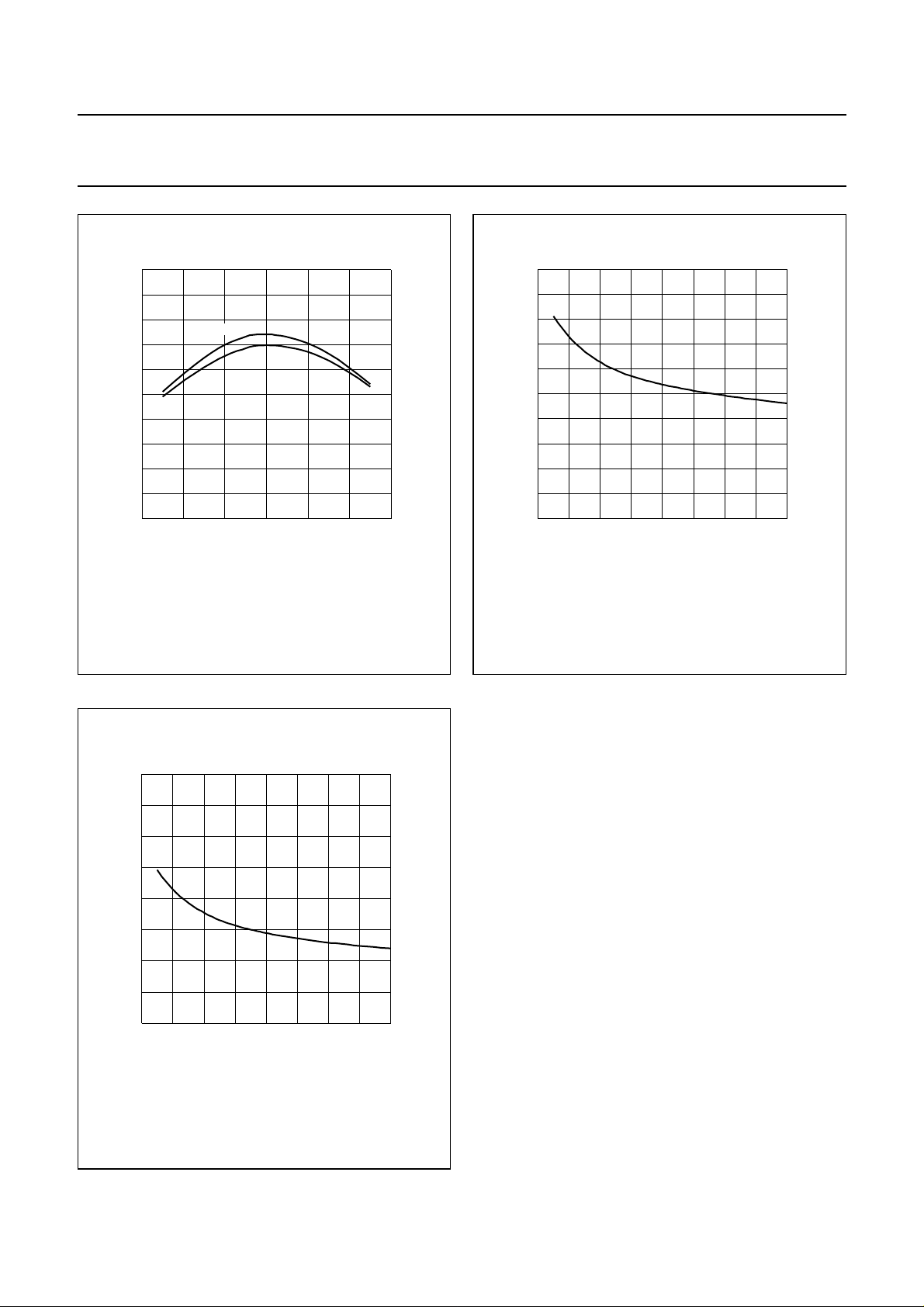
Fig.7 Gain and efficiency as functions of load
power, typical values.
3
P
(W)
D
MRA551
4
100
η
C
(%)
80
60
40
20
0
16
16
handbook, halfpage
P
L
(W)
12
8
4
0
012
Class-AB operation; VCE= 12.5 V; f = 900 MHz;
=10mA.
I
CQ
Fig.8 Load power as a function of drive power,
typical values.
March 1993 6
Ruggedness in class-AB operation
The BLV193 is capable of withstanding a load mismatch
corresponding to VSWR = 10:1 through all phases under
the following conditions:
VCE= 15.5 V, f = 900 MHz,
Th=25°C, R
= 0.4 K/W, and
th j-mb
rated output power.
Page 7

Philips Semiconductors Product specification
UHF power transistor BLV193
16
handbook, halfpage
G
p
(dB)
12
8
4
0
048
Class-A operation; VCE= 12 V; IC= 1.3 A;
= 900 MHz; fq= 901 MHz.
f
p
MRA558
P
(W)
L(PEP)
Fig.9 Gain as a function of load power (PEP),
typical values.
12
handbook, halfpage
P
L(PEP)
(W)
10
8
6
4
2
0
12
0 0.2 0.4 0.6
Class-A operation; VCE= 12 V; IC= 1.3 A;
= 900 MHz; fq= 901 MHz.
f
p
MRA550
0.8 1
P
D(PEP)
(W)
Fig.10 Load power (PEP) as a function of drive
power (PEP), typical values.
handbook, halfpage
0
d3, d
5
(dB)
−10
−20
−30
−40
−50
−60
−70
04
Class-A operation; VCE= 12 V; IC= 1.3 A;
= 900 MHz; fq= 901 MHz.
f
p
d
3
d
5
812
MRA560
P
(W)
L(PEP)
Fig.11 Intermodulation products as a function of
load power (PEP), typical values.
March 1993 7
Page 8

Philips Semiconductors Product specification
UHF power transistor BLV193
handbook, full pagewidth
50 Ω
C1
C6
L6
L5
L4
C7
L9
C13
L1 L2
C2 C3 C4
C16
V
bias
C5
L3
L8
R1 L10
DUT
Fig.12 Class-A and class-AB test circuit at f = 900 MHz.
C8
L7
C9 C10 C11
L11
R2
C12
C14 C15
MBC797
+V
50 Ω
CC
March 1993 8
Page 9

Philips Semiconductors Product specification
UHF power transistor BLV193
List of components (see test circuit)
COMPONENT DESCRIPTION VALUE DIMENSIONS CATALOGUE NO.
C1, C12 multilayer ceramic chip capacitor
(note 1)
C2, C3, C10, C11 film dielectric trimmer 1.4 to 5.5 pF 2222 809 09001
C4, C5 multilayer ceramic chip capacitor
(note 1)
C6, C7 multilayer ceramic chip capacitor
(note 1)
C8, C9 multilayer ceramic chip capacitor
(note 1)
C13 multilayer ceramic chip capacitor
(note 1)
C14 electrolytic capacitor 6.8 µF, 63 V
C15 multilayer ceramic chip capacitor
(note 1)
C16 multilayer ceramic chip capacitor 100 nF 2222 852 47104
L1, L7 stripline (note 2) 50 Ω length 29 mm;
L2 stripline (note 2) 50 Ω length 6 mm;
L3 stripline (note 2) 42.7 Ω length 13.1 mm;
L4 stripline (note 2) 42.7 Ω length 4.4 mm;
L5 stripline (note 2) 42.7 Ω length 4.6 mm;
L6 stripline (note 2) 50 Ω length 7 mm;
L8 4 turns closely wound enamelled
0.4 mm copper wire
L9 4 turns enamelled 1 mm copper
wire
L10, L11 grade 3B Ferroxcube wideband HF
choke
R1, R2 metal film resistor 10 Ω, 0.25 W
33 pF
4.7 pF
5.6 pF
3.3 pF
10 pF
330 pF
width 2.4 mm
width 2.4 mm
width 3 mm
width 3 mm
width 3 mm
width 2.4 mm
60 nH int. dia 3 mm;
leads 2 × 5mm
45 nH int. dia. 4 mm;
leads 2 × 5mm
4312 020 36642
Notes
1. American Technical Ceramics type 100A or capacitor of the same quality.
2. The striplines are on a double copper-clad printed circuit board, with PTFE fibre-glass dielectric (ε
thickness1⁄32inch.
March 1993 9
= 2.2),
r
Page 10

Philips Semiconductors Product specification
UHF power transistor BLV193
handbook, full pagewidth
handbook, full pagewidth
124 mm
80 mm
MBC798
V
bias
V
CC
L10
C13
C16 R1
C1
The components are mounted on one side of a copper clad PTFE fibre-glass board; the other side is unetched
and serves as a ground plane. Earth connections from the component side to the ground plane are made by
fixing screws and copper straps under the emitter leads.
L1
C2
C5
L2
C4
L8
L3
C6
L4
L5
C7
R2
L9
C8
L6
C9
C10C3
C15
L7
Fig.13 Printed circuit board and component layout for 900 MHz test circuit.
C14L11
C12
C11
MBC799
March 1993 10
Page 11

Philips Semiconductors Product specification
UHF power transistor BLV193
handbook, halfpage
5
Z
i
(Ω)
4
x
i
3
2
1
0
840 880
Class-AB operation; VCE= 12.5 V; ICQ=10mA;
= 12 W; Th=25°C.
P
L
r
i
920 960
MRA561
f (MHz)
Fig.14 Input impedance (series components) as a
function of frequency, typical values.
handbook, halfpage
5
Z
L
(Ω)
4
R
L
3
X
2
1
0
840 880
Class-AB operation; VCE= 12.5 V; ICQ=10mA;
= 12 W; Th=25°C.
P
L
L
920 960
MRA548
f (MHz)
Fig.15 Load impedance (series components) as a
function of frequency, typical values.
handbook, halfpage
Z
i
Z
MBA451
L
Fig.16 Definition of transistor impedance.
March 1993 11
10
handbook, halfpage
G
p
(dB)
8
6
4
2
0
840 880
Class-AB operation; VCE= 12.5 V; ICQ=10mA;
= 12 W; Th=25°C.
P
L
920 960
f (MHz)
Fig.17 Power gain as a function of frequency,
typical values.
MRA556
Page 12

Philips Semiconductors Product specification
UHF power transistor BLV193
x
i
r
i
f (MHz)
MRA547
handbook, halfpage
5
Z
i
(Ω)
4
3
2
1
0
840 880
Class-A operation; VCE= 12 V; IC= 1.3 A;
=25°C.
T
h
920 960
Fig.18 Input impedance (series components) as a
function of frequency, typical values.
handbook, halfpage
5
Z
L
(Ω)
4
3
2
1
0
840 880
Class-A operation; VCE= 12 V; IC= 1.3 A;
=25°C.
T
h
R
L
X
L
920 960
MRA549
f (MHz)
Fig.19 Load impedance (series components) as a
function of frequency, typical values.
handbook, halfpage
Z
i
Z
L
Fig.20 Definition of transistor impedance.
MBA451
14
handbook, halfpage
G
p
(dB)
12
8
4
0
840 880 920
Class-A operation; VCE= 12 V; IC= 1.3 A;
=25°C.
T
h
f (MHz)
Fig.21 Power gain as a function of frequency,
typical values.
MRA557
960
March 1993 12
Page 13

Philips Semiconductors Product specification
UHF power transistor BLV193
PACKAGE OUTLINE
Flanged ceramic package; 2 mounting holes; 6 leads SOT171A
D
A
F
D
1
U
1
q
H
1
b
1
2
H
U
2
Db
9.25
9.04
0.364
0.356
1
D
1
9.30
8.99
0.366
0.354
5.95
5.74
0.234
0.226
A
DIMENSIONS (millimetre dimensions are derived from the original inch dimensions)
UNIT
mm
inches
A
6.81
6.07
0.268
0.239
2.15
1.85
0.085
0.073
b
1
3.20
2.89
0.126
0.114
c
0.16
0.07
0.006
0.003
6
345
b
e
0 5 10 mm
E
E
1
6.00
5.70
0.236
0.224
e
3.58
0.140
C
w
M
C
2
p
w
M
3
scale
F
H
11.31
3.05
10.54
2.54
0.445
0.120
0.415
0.100
w
H
9.27
9.01
0.365
0.355
B
1
c
E
1
M
AB
1
Q
qw
18.42
U
1
24.90
24.63
0.980
0.970
6.00
5.70
0.236
0.224
p
3.43
3.17
0.135
0.125
Q
4.32
4.11
0.170
0.162
E
w
U
2
2
1
w
3
0.260.51 1.02
0.010.02 0.040.725
OUTLINE
VERSION
SOT171A 97-06-28
IEC JEDEC EIAJ
REFERENCES
EUROPEAN
PROJECTION
March 1993 13
ISSUE DATE
Page 14

Philips Semiconductors Product specification
UHF power transistor BLV193
DEFINITIONS
Data Sheet Status
Objective specification This data sheet contains target or goal specifications for product development.
Preliminary specification This data sheet contains preliminary data; supplementary data may be published later.
Product specification This data sheet contains final product specifications.
Limiting values
Limiting values given are in accordance with the Absolute Maximum Rating System (IEC 134). Stress above one or
more of the limiting values may cause permanent damage to the device. These are stress ratings only and operation
of the device at these or at any other conditions above those given in the Characteristics sections of the specification
is not implied. Exposure to limiting values for extended periods may affect device reliability.
Application information
Where application information is given, it is advisory and does not form part of the specification.
LIFE SUPPORT APPLICATIONS
These products are not designed for use in life support appliances, devices, or systems where malfunction of these
products can reasonably be expected to result in personal injury. Philips customers using or selling these products for
use in such applications do so at their own risk and agree to fully indemnify Philips for any damages resulting from such
improper use or sale.
March 1993 14
 Loading...