

Page 1

DISCRETE SEMICONDUCTORS
DATA SH EET
BLT50
UHF power transistor
Product specification
April 1991
Page 2
Philips Semiconductors Product specification
UHF power transistor BLT50
FEATURES
• SMD encapsulation
• Gold metallization ensures
excellent reliability.
DESCRIPTION
NPN silicon planar epitaxial transistor
encapsulated in a SOT223 surface
mounted envelope and designed
primarily for use in hand-held radio
equipment in the 470 MHz
communications band.
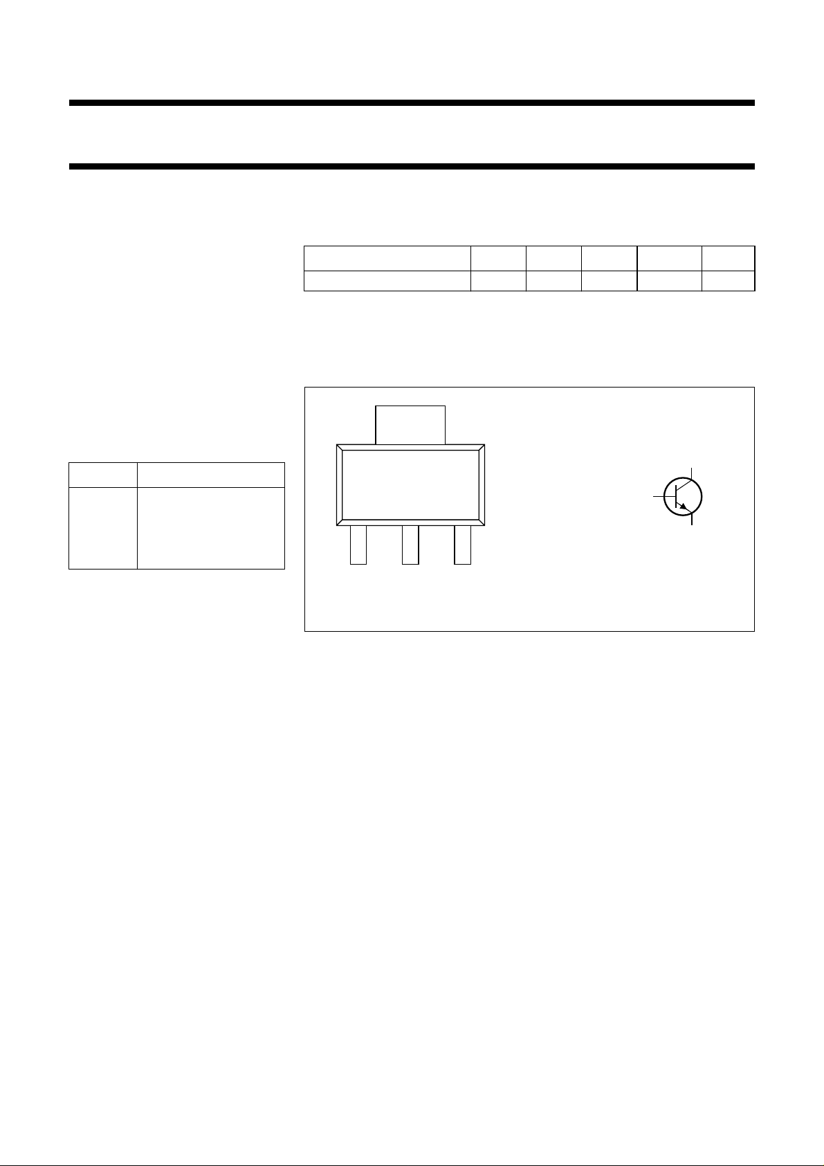
PINNING - SOT223
PIN DESCRIPTION
1 emitter
2 base
3 emitter
4 collector
QUICK REFERENCE DATA
RF performance at T
≤ 60 °C in a common emitter class-B test circuit
s
(note 1).
MODE OF OPERATION f (MHz) V
(V) PL (W) Gp (dB) ηc (%)
CE
c.w. narrow band 470 7.5 1.2 > 10 > 55
Note
1. T
= temperature at soldering point of collector tab.
s
PIN CONFIGURATION
ge
123
Top view
4
MSB002 - 1
handbook, halfpage
MBB012
c
b
e
Fig.1 Simplified outline and symbol.
April 1991 2
Page 3
Philips Semiconductors Product specification
UHF power transistor BLT50
LIMITING VALUES
In accordance with the Absolute Maximum System (IEC 134).
SYMBOL PARAMETER CONDITIONS MIN. MAX. UNIT
V
CBO
V
CEO
V
EBO
I
, I
C
C(AV)
I
CM
P
tot
T
stg
T
j
Note
= temperature at soldering point of collector tab.
1. T
s
collector-base voltage open emitter − 20 V
collector-emitter voltage open base − 10 V
emitter-base voltage open collector − 3V
collector current DC or average value − 500 mA
collector current peak value
− 1.5 A
f > 1 MHz
total power dissipation f > 1 MHz;
− 2W
Ts = 103 °C
(note 1)
storage temperature range −65 150 °C
operating junction temperature − 175 °C
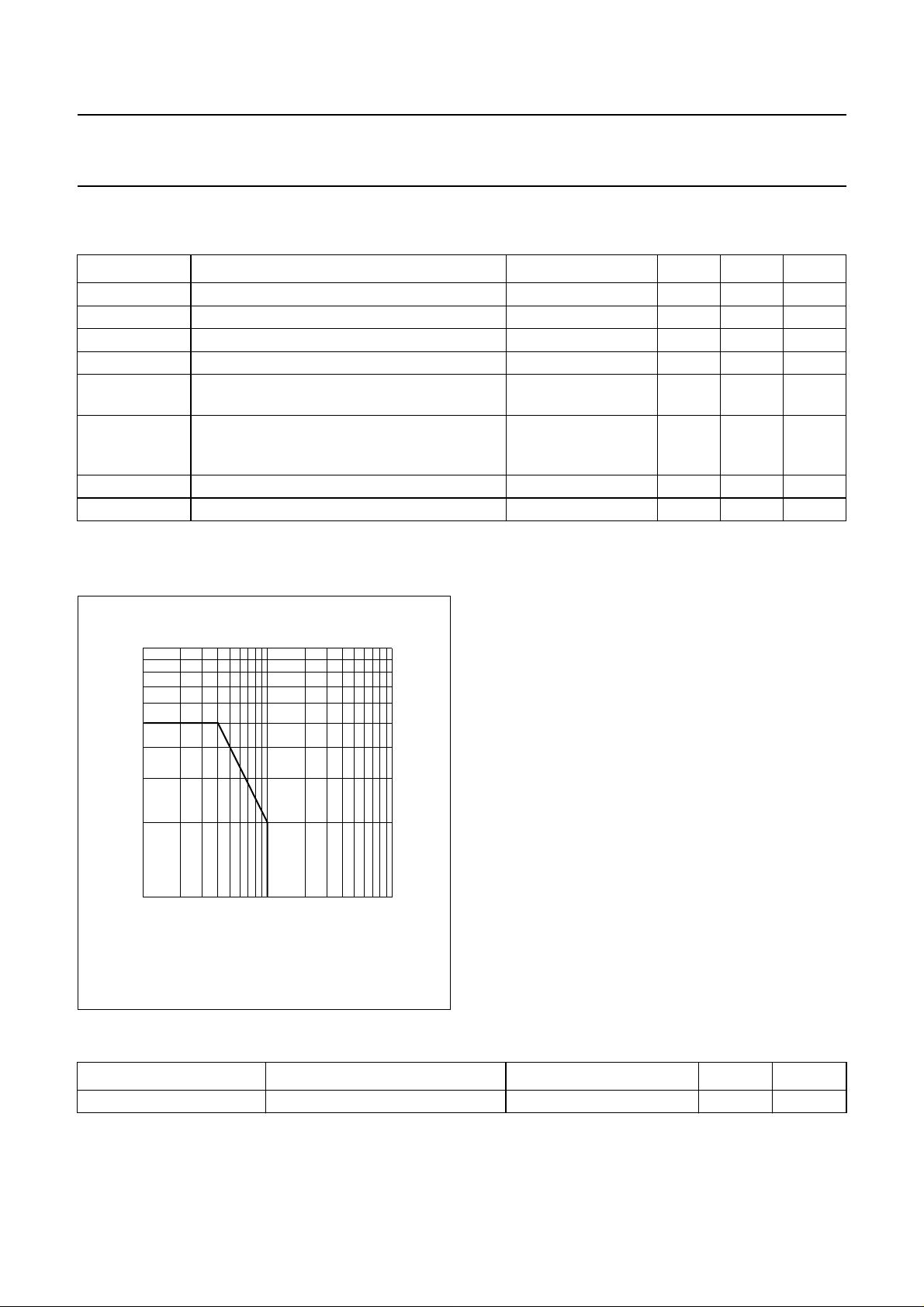
handbook, halfpage
1
I
C
(A)
0.5
0.2
0.1
1
Ts= 103°C.
Fig.2 DC SOAR.
THERMAL RESISTANCE
SYMBOL PARAMETER CONDITIONS MAX. UNIT
R
th j-s(DC)
MEA217
2
10
VCE (V)
10
from junction to soldering point P
= 2 W; Ts = 103 °C 36 K/W
tot
April 1991 3
Page 4

Philips Semiconductors Product specification
UHF power transistor BLT50
CHARACTERISTICS
T
= 25 °C.
j
SYMBOL PARAMETER CONDITIONS MIN. TYP. MAX. UNIT
V
(BR)CBO
V
(BR)CEO
V
(BR)EBO
I
CES
h
FE
E
SBR
C
c
C
re
collector-base breakdown voltage open emitter;
IC = 5 mA
collector-emitter breakdown voltage open base;
IC = 10 mA
emitter-base breakdown voltage open collector;
IE = 1 mA
collector-emitter leakage current VBE = 0;
VCE = 10 V
DC current gain VCE = 5 V;
IC = 300 mA
second breakdown energy L = 25 mH;
RBE = 10 Ω;
f = 50 Hz
collector capacitance VCB = 7.5 V;
IE = Ie = 0;
f = 1 MHz
feedback capacitance VCE = 7.5 V;
IC = 0;
f = 1 MHz
20 −−V
10 −−V
3 −−V
−−250 µA
25 −−
0.55 −−mJ
− 4.7 6 pF
− 2.9 4.5 pF
10
handbook, halfpage
C
c
(pF)
8
6
4
2
0
0810
IE=ie= 0; f = 1 MHz.
246
VCB (V)
Fig.3 Collector capacitance as a function of
collector-base voltage, typical values.
MEA218
April 1991 4
Page 5

Philips Semiconductors Product specification
UHF power transistor BLT50
APPLICATION INFORMATION
RF performance at T
≤ 60 °C in a common emitter class-B test circuit.
s
MODE OF
OPERATION
f (MHz) V
(V) PL (W) Gp (dB) ηc (%)
CE
c.w. narrow band 470 7.5 1.2 > 10
typ. 11.2
16
handbook, halfpage
G
p
(dB)
12
8
4
0
0.6 1.0 1.4 2.21.8
MEA219
100
η
G
p
(%)
80
handbook, halfpage
η
60
40
PL (W)
2
P
L
(W)
1
0
0 100
PD (mW)
> 55
typ. 65
MEA220
200
VCE = 7.5 V; f = 470 MHz.
Fig.4 Gain and efficiency as functions of load
power, typical values.
Ruggedness in class-B operation
The BLT50 is capable of withstanding a load mismatch
corresponding to VSWR = 50:1 through all phases at rated
output power, up to a supply voltage of 9 V, f = 470 MHz
and Ts≤ 60 °C, where Ts is the temperature at the
soldering point of the collector tab.
VCE = 7.5 V; f = 470 MHz.
Fig.5 Load power as a function of drive power,
typical values.
April 1991 5
Page 6

Philips Semiconductors Product specification
UHF power transistor BLT50
handbook, full pagewidth
C1
50 Ω 50 Ω
C2
R1
L1
TUT
L2
L3
L5L4
L6
L7
R2
C3
C4
C7C6C5
+V
CC
MBA576
Fig.6 Class-B test circuit at f = 470 MHz.
List of components (see test circuit)
COMPONENT DESCRIPTION VALUE DIMENSIONS CATALOGUE NO.
C1 film dielectric trimmer 1.4 to 5.5 pF 2222 809 09004
C2 film dielectric trimmer 1.4 to 5.5 pF 2222 809 09001
C3 film dielectric trimmer 2 to 9 pF 2222 809 09002
C4 film dielectric trimmer 2 to 9 pF 2222 809 09005
C5 multilayer ceramic chip capacitor
100 pF
(note 1)
C6 multilayer ceramic chip capacitor
1 nF
(note 1)
C7 63 V electrolytic capacitor 2.2 µF
L1 stripline (note 2) 50 Ω 54 mm × 4.7 mm
L2 5 turns enamelled 0.4 mm copper
int. dia. 3 mm
wire
L3, L7 grade 3B1 Ferroxcube wideband RF
4312 020 36640
choke
L4 stripline (note 2) 50 Ω 36 mm × 4.7 mm
L5 1 turn enamelled 1.4 mm copper wire 5 nH int. dia. 4 mm
L6 3 turns enamelled 0.4 mm copper
int. dia. 3 mm
wire
R1, R2 0.25 W metal film resistor 10 Ω,5%
Notes
1. American Technical Ceramics (ATC) capacitor, type 100B or other capacitor of the same quality.
2. The striplines are mounted on a double copper-clad printed circuit board, with PTFE fibre-glass dielectric (ε
thickness1⁄16inch.
April 1991 6
= 2.2);
r
Page 7

Philips Semiconductors Product specification
UHF power transistor BLT50
handbook, full pagewidth
V
CC
L3
L7
C7
handbook, full pagewidth
C1 C2
strap
C5
R1
L2
L1
140 mm
L4
R2
L6
C6
C3
L5
C4
MBA575
strap
rivets
(14x)
strap
The circuit and components are situated on one side of a copper-clad PTFE fibre-glass board; the other side is
unetched and serves as a ground plane. Earth connections from the component side to the ground plane are
made by means of fixing screws, hollow rivets and copper foil straps, as shown.
mounting
screws
(8x)
Fig.7 Component layout for 470 MHz class-B test circuit.
April 1991 7
80 mm
strap
MBA574
Page 8

Philips Semiconductors Product specification
UHF power transistor BLT50
handbook, halfpage
4
Z
i
(Ω)
3
2
1
0
350 450
Class-B operation; VCE = 7.5 V; PL = 1.2 W.
r
i
x
i
550 650
MEA221
f (MHz)
Fig.8 Input impedance (series components) as a
function of frequency, typical values.
20
handbook, halfpage
Z
L
(Ω)
15
10
5
0
350 450 550
Class-B operation; VCE = 7.5 V; PL = 1.2 W.
X
L
R
L
MEA222
f (MHz)
Fig.9 Load impedance (series components) as a
function of frequency, typical values.
650
handbook, halfpage
Z
i
Z
MBA451
L
Fig.10 Definition of transistor impedance.
April 1991 8
16
handbook, halfpage
G
p
(dB)
12
8
4
0
350 450 550
Class-B operation; VCE = 7.5 V; PL = 1.2 W.
f (MHz)
Fig.11 Power gain as a function of frequency,
typical values.
MEA223
650
Page 9

Philips Semiconductors Product specification
UHF power transistor BLT50
PACKAGE OUTLINE
Plastic surface mounted package; collector pad for good heat transfer; 4 leads SOT223
D
c
y
b
1
4
132
e
1
b
p
e
w M
B
E
H
E
A
1
detail X
AB
X
v M
A
Q
A
L
p
0 2 4 mm
scale
DIMENSIONS (mm are the original dimensions)
UNIT A1b
mm
A
1.8
1.5
OUTLINE
VERSION
SOT223
0.10
0.01
cD
b
p
1
0.80
3.1
0.32
0.60
2.9
IEC JEDEC EIAJ
0.22
6.7
6.3
e
E
3.7
4.6
3.3
REFERENCES
e1HELpQywv
2.3
April 1991 9
7.3
6.7
1.1
0.7
0.95
0.85
0.1 0.10.2
EUROPEAN
PROJECTION
ISSUE DATE
96-11-11
97-02-28
Page 10

Philips Semiconductors Product specification
UHF power transistor BLT50
DEFINITIONS
Data Sheet Status
Objective specification This data sheet contains target or goal specifications for product development.
Preliminary specification This data sheet contains preliminary data; supplementary data may be published later.
Product specification This data sheet contains final product specifications.
Limiting values
Limiting values given are in accordance with the Absolute Maximum Rating System (IEC 134). Stress above one or
more of the limiting values may cause permanent damage to the device. These are stress ratings only and operation
of the device at these or at any other conditions above those given in the Characteristics sections of the specification
is not implied. Exposure to limiting values for extended periods may affect device reliability.
Application information
Where application information is given, it is advisory and does not form part of the specification.
LIFE SUPPORT APPLICATIONS
These products are not designed for use in life support appliances, devices, or systems where malfunction of these
products can reasonably be expected to result in personal injury. Philips customers using or selling these products for
use in such applications do so at their own risk and agree to fully indemnify Philips for any damages resulting from such
improper use or sale.
April 1991 10
 Loading...