

Page 1

DISCRETE SEMICONDUCTORS
DATA SH EET
BLF543
UHF power MOS transistor
Product specification
October 1992
Page 2
Philips Semiconductors Product specification
UHF power MOS transistor BLF543
FEATURES
• High power gain
• Easy power control
• Good thermal stability
• Gold metallization ensures
excellent reliability
• Designed for broadband operation.
DESCRIPTION
Silicon N-channel enhancement
mode vertical D-MOS transistor
designed for communications
transmitter applications in the UHF
frequency range.
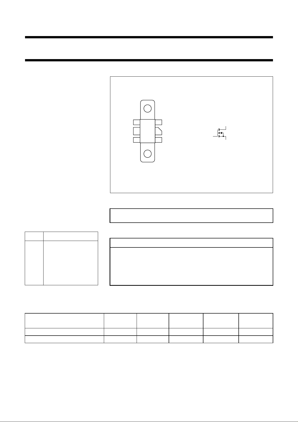
The transistor is encapsulated in a
6-lead, SOT171 flange envelope, with
a ceramic cap. All leads are isolated
from the flange.
The devices are marked with a
V
indication intended for matched
GS
pair applications.
PINNING - SOT171
PIN DESCRIPTION
1 source
2 source
3 gate
4 drain
5 source
6 source
PIN CONFIGURATION
page
1
3
5
Top view
2
4
6
MBA931 - 1
g
MBB072
d
s
Fig.1 Simplified outline and symbol.
CAUTION
The device is supplied in an antistatic package. The gate-source input must
be protected against static charge during transport and handling.
WARNING
Product and environmental safety - toxic materials
This product contains beryllium oxide. The product is entirely safe provided
that the BeO disc is not damaged. All persons who handle, use or dispose of
this product should be aware of its nature and of the necessary safety
precautions. After use, dispose of as chemical or special waste according to
the regulations applying at the location of the user. It must never be thrown
out with the general or domestic waste.
QUICK REFERENCE DATA
RF performance at T
MODE OF OPERATION
= 25 °C in a common source class-B circuit.
h
f
(MHz)
V
(V)
DS
P
(W)
L
G
p
(dB)
η
(%)
CW, class-B 500 28 10 > 12 > 50
CW, class-B 960 28 10 typ. 8 typ. 50
October 1992 2
D
Page 3
Philips Semiconductors Product specification
UHF power MOS transistor BLF543
LIMITING VALUES
In accordance with the Absolute Maximum System (IEC 134).
SYMBOL PARAMETER CONDITIONS MIN. MAX. UNIT
V
DS
±V
GS
I
D
P
tot
T
stg
T
j
THERMAL RESISTANCE
SYMBOL PARAMETER THERMAL RESISTANCE
R
th j-mb
R
th mb-h
drain-source voltage − 65 V
gate-source voltage − 20 V
DC drain current − 2A
total power dissipation up to Tmb=25°C − 25 W
storage temperature −65 150 °C
junction temperature − 200 °C
thermal resistance from junction to mounting base 7 K/W
thermal resistance from mounting base to heatsink 0.4 K/W
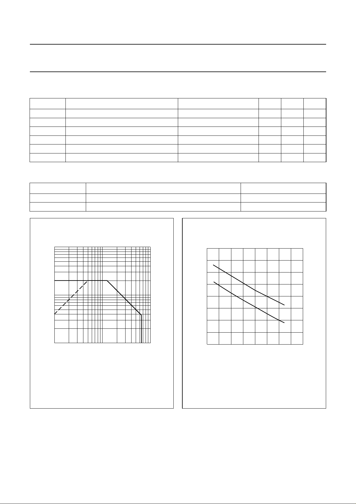
10
handbook, halfpage
I
D
(A)
1
−1
10
(1) Current in this area may be limited by R
(2) Tmb=25°C.
(1)
11010
Fig.2 DC SOAR.
(2)
VDS (V)
.
DS(on)
MRA991
2
40
handbook, halfpage
P
tot
(W)
30
20
10
0
0 40 80 160
(1) Continuous operation.
(2) Short-time operation during mismatch.
(1)
(2)
Fig.3 Power/temperature derating curves.
120
MDA488
Th (°C)
October 1992 3
Page 4
Philips Semiconductors Product specification
UHF power MOS transistor BLF543
CHARACTERISTICS
T
= 25 °C unless otherwise specified.
j
SYMBOL PARAMETER CONDITIONS MIN. TYP. MAX. UNIT
V
(BR)DSS
I
DSS
I
GSS
V
GS(th)
∆V
GS(th)
g
fs
R
DS(on)
I
DSX
C
is
C
os
C
rs
drain-source breakdown voltage VGS= 0; ID = 5 mA 65 −−V
drain-source leakage current VGS= 0; VDS= 28 V −−0.5 mA
gate-source leakage current ±VGS= 20 V; VDS=0 −−1µA
gate-source threshold voltage ID= 20 mA; VDS= 10 V 1 − 4V
gate-source voltage difference of
ID= 20 mA; VDS= 10 V −−100 mV
matched pairs
forward transconductance ID= 0.6 A; VDS= 10 V 300 450 − mS
drain-source on-state resistance ID= 0.6 A; VGS= 10 V − 1.7 2.5 Ω
on-state drain current VGS= 15 V; VDS= 10 V − 2.4 − A
input capacitance VGS= 0; VDS= 28 V; f = 1 MHz − 16 − pF
output capacitance VGS= 0; VDS= 28 V; f = 1 MHz − 12 − pF
feedback capacitance VGS= 0; VDS= 28 V; f = 1 MHz − 3.2 − pF
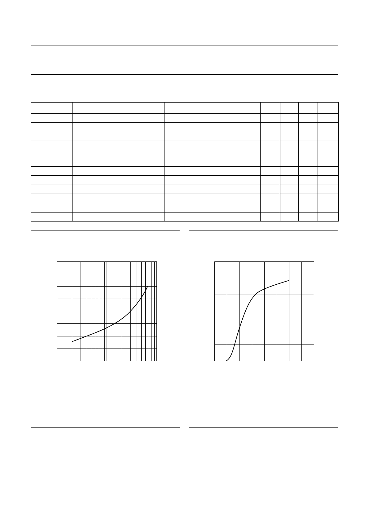
handbook, halfpage
4
T.C.
(mV/K)
2
0
−2
−4
10
VDS= 10 V.
−2
−1
10
ID (A)
Fig.4 Temperature coefficient of gate-source
voltage as a function of drain current, typical
values.
MDA491
handbook, halfpage
1
3
I
D
(A)
2
1
0
0
VDS= 10 V; Tj= 25 °C.
5
10 20
MDA495
15
V
(V)
GS
Fig.5 Drain current as a function of gate-source
voltage, typical values.
October 1992 4
Page 5
Philips Semiconductors Product specification
UHF power MOS transistor BLF543
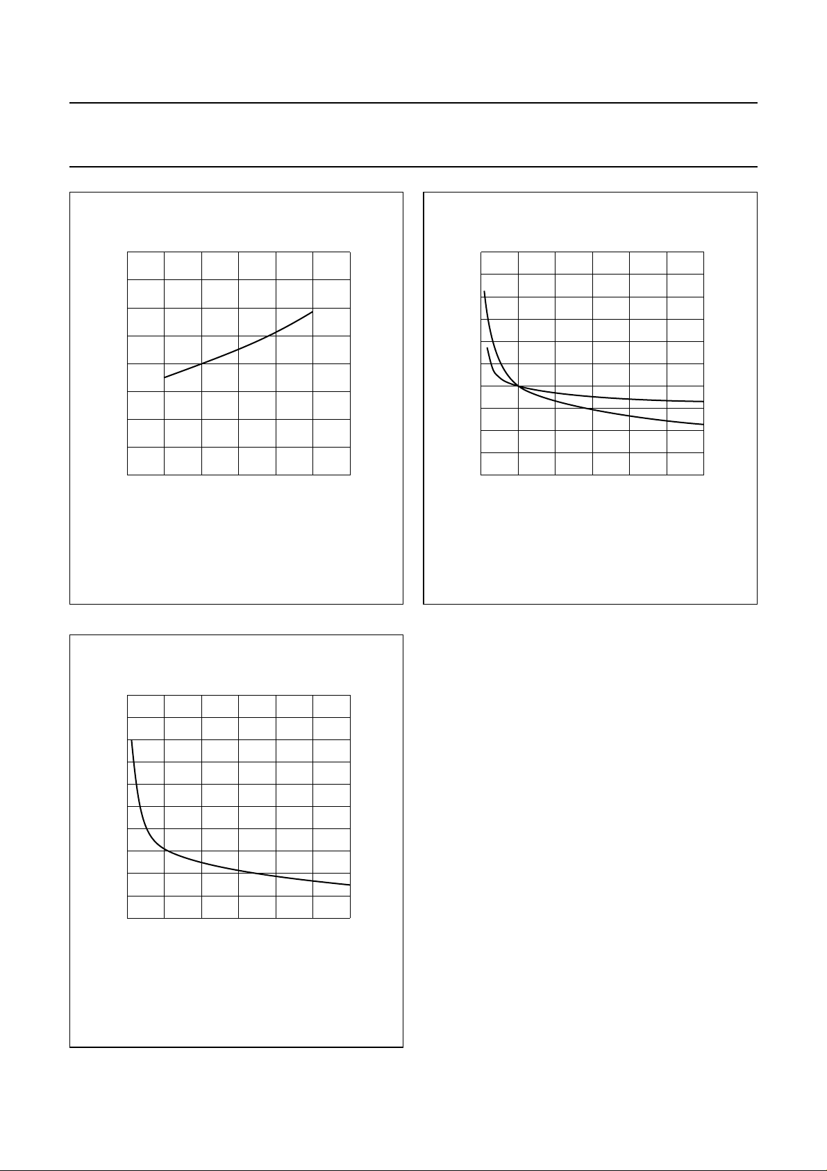
handbook, halfpage
4
R
DSon
(Ω)
3
2
1
0
0 50 100 150
ID= 0.6 A; VGS= 10 V.
Tj ( °C)
Fig.6 Drain-source on-state resistance as a
function of junction temperature, typical
values.
MDA496
50
handbook, halfpage
C
(pF)
40
30
20
10
0
010
VGS= 0; f = 1 MHz.
20 30
MDA497
C
is
C
os
V
(V)
DS
Fig.7 Input and output capacitance as functions
of drain-source voltage, typical values.
20
handbook, halfpage
C
rs
(pF)
16
12
8
4
0
010
VGS= 0; f = 1 MHz.
20 30
MDA498
V
(V)
DS
Fig.8 Feedback capacitance as a function of
drain-source voltage, typical values.
October 1992 5
Page 6

Philips Semiconductors Product specification
UHF power MOS transistor BLF543
APPLICATION INFORMATION FOR CLASS-B OPERATION
T
= 25 °C; R
h
RF performance in a common source class-B circuit.
= 0.4 K/W, unless otherwise specified.
th mb-h
MODE OF OPERATION
f
(MHz)
CW class-B 500 28 20 10 > 12
V
(V)
DS
I
DQ
(mA)
P
(W)
L
G
p
(dB)
η
(%)
> 50
typ. 15
typ. 60
CW class-B 960 28 20 10 typ. 8 typ. 50
CW class-B 960 24 20 7.5 typ. 8 typ. 50
Ruggedness in class-B operation
The BLF543 is capable of withstanding a full load
mismatch corresponding to VSWR = 50 through all phases
under the following conditions:
VDS= 28 V; f = 500 MHz at rated output power.
30
handbook, halfpage
G
p
(dB)
20
MDA490
80
η
D
η
(%)
G
p
D
60
15
handbook, halfpage
P
L
(W)
10
MDA489
D
10
0
0
Class-B operation; VDS= 28 V; IDQ= 20 mA;
= 8.4+ j14.3 Ω; f = 500 MHz.
Z
L
5
10 15
PL (W)
40
20
Fig.9 Power gain and efficiency as functions of
load power, typical values.
October 1992 6
5
0
0
Class-B operation; VDS= 28 V; IDQ= 20 mA;
= 8.4 + j14.3 Ω; f = 500 MHz.
Z
L
0.5
1 1.5
PIN (W)
Fig.10 Load power as a function of input power,
typical values.
Page 7

Philips Semiconductors Product specification
UHF power MOS transistor BLF543
handbook, full pagewidth
50 Ω
input
C1
C2
C3
C12
L8
C13
C9
BLF543
L6 R5
L4
L7
L5
C10
C11
C4
L1
L2 L3
C5
C6
C7
D.U.T.
R1
C8
R2
C14
C16
C15
50 Ω
output
+V
R3 R4
D
Fig.11 Test circuit for class-B operation at 500 MHz.
MDA500
October 1992 7
Page 8

Philips Semiconductors Product specification
UHF power MOS transistor BLF543
List of components (class-B test circuit at 500 MHz)
COMPONENT DESCRIPTION VALUE DIMENSIONS CATALOGUE NO.
C1, C6, C9, C16 multilayer ceramic chip capacitor
(note 1)
C2, C14 multilayer ceramic chip capacitor
(note 1)
C3, C5, C13, C15 film dielectric trimmer 9 pF 2222 809 09002
C4 multilayer ceramic chip capacitor
(note 1)
C7 multilayer ceramic chip capacitor 2 × 100 nF in
C8, C10 multilayer ceramic chip capacitor 100 nF 2222 852 47104
C11 aluminium electrolytic capacitor 10 µF, 63 V 2222 030 28109
C12 multilayer ceramic chip capacitor
(note 1)
L1 1 turn enamelled 0.8 mm copper
wire
L2 stripline (note 2) 42.5 Ω 14.5 × 3 mm
L3, L4 stripline (note 2) 42.5 Ω 6 × 3 mm
L5 7 turns enamelled 1 mm copper
wire
L6 grade 3B Ferroxcube RF choke 4312 020 36640
L7 stripline (note 2) 55.7 Ω 31 × 2 mm
L8 1 turn enamelled 1 mm copper wire 8 nH int. dia. 3.2 mm
R1, R2 0.4 W metal film resistor 1 kΩ 2322 151 71002
R3 10 turns cermet potentiometer 5 kΩ
R4 0.4 W metal film resistor 19.6 kΩ 2322 151 71963
R5 1 W metal film resistor 10 Ω 2322 153 51009
390 pF
7.5 pF
20 pF
2222 852 47104
parallel, 50 V
22 pF
11 nH int. dia. 4.7 mm
leads 2 × 5 mm
124 nH length 7.8 mm
int. dia. 4 mm
leads 2 × 5 mm
leads 2 × 5 mm
Notes
1. American Technical Ceramics (ATC) capacitor, type 100B or other capacitor of the same quality.
2. The striplines are on a double copper-clad printed circuit board, with glass microfibre reinforced PTFE (ε
thickness1⁄32inch.
October 1992 8
= 2.2);
r
Page 9

Philips Semiconductors Product specification
UHF power MOS transistor BLF543
handbook, full pagewidth
mounting screw
+V
6
mm
rivet
strapstrap
G
R4
R5
+V
D
52 mm 59 mm
R3
70 mm
C7
R2
C4C2
C1
The circuit and components are situated on one side of the printed circuit board, the other side being fully
metallized, to serve as a ground plane. Earth connections are made by means of copper straps and hollow rivets
for a direct contact between upper and lower sheets.
L1
L2 L7
C8
C6
R1
BLF543
C9
L4L3
L6
L5
C10
C12
C13 C15C3 C5
Fig.12 Component layout for 500 MHz class-B test circuit.
C11
C14
L8 C16
MDA487
October 1992 9
Page 10

Philips Semiconductors Product specification
UHF power MOS transistor BLF543
handbook, full pagewidth
C14
L5
L6
L8 L9L8
C10
C11
C17
C16C15
50 Ω
output
50 Ω
input
L1 L2 L3
C1
C3
C4
C5
R3
C6C2
L4
C7
C8
D.U.T.
BLF543
C9
R2 R1
R4 L10
C12
C13
+V
D
MDA499
Fig.13 Test circuit for class-B operation at 960 MHz.
October 1992 10
Page 11

Philips Semiconductors Product specification
UHF power MOS transistor BLF543
List of components (class-B test circuit at 960 MHz)
COMPONENT DESCRIPTION VALUE DIMENSIONS CATALOGUE NO.
C1, C8, C10, C17 multilayer ceramic chip capacitor
(note 1)
C2 multilayer ceramic chip capacitor
(note 2)
C3, C5, C15, C16 film dielectric trimmer 1.2 to 5.5 pF 2222 808 00004
C4 multilayer ceramic chip capacitor
(note 2)
C6, C7 multilayer ceramic chip capacitor
(note 2)
C9, C12 multilayer ceramic chip capacitor 100 nF 2222 852 47104
C14 multilayer ceramic chip capacitor
(note 2)
C11, C13 aluminum electrolytic capacitor 10 µF, 63 V 2222 030 28109
L1 stripline (note 3) 50 Ω 12.5 × 2.5 mm
L2 stripline (note 3) 50 Ω 19 × 2.5 mm
L3 stripline (note 3) 50 Ω 29.5 × 2.5 mm
L4, L5 stripline (note 3) 42.5 Ω 3 × 3 mm
L6 3 turns enamelled 0.8 mm copper
wire
L7 stripline (note 3) 50 Ω 12.5 × 2.5 mm
L8 stripline (note 3) 50 Ω 28.5 × 2.5 mm
L9 stripline (note 3) 50 Ω 20.5 × 2.5 mm
L10 grade 3B Ferroxcube RF choke 4312 020 36640
R1 0.4 W metal film resistor 205 kΩ 2322 151 72054
R2 10 turns potentiometer 50 kΩ
R3 0.4 W metal film resistor 10 kΩ 2322 151 71003
R4 0.4 W metal film resistor 10 Ω 2322 153 51009
68 pF
4.7 pF
2 × 5.6 pF in
parallel
7.5 pF
2 × 4.7 pF in
parallel
35 nH length 4.6 mm
int. dia. 4 mm
leads 2 × 5 mm
Notes
1. American Technical Ceramics (ATC) capacitor, type 100B or other capacitor of the same quality.
2. American Technical Ceramics (ATC) capacitor, type 100A or other capacitor of the same quality.
3. The striplines are on a double copper-clad printed circuit board, with glass microfibre reinforced PTFE (ε
thickness1⁄32inch.
October 1992 11
= 2.2);
r
Page 12

Philips Semiconductors Product specification
UHF power MOS transistor BLF543
10
handbook, halfpage
Z
i
(Ω)
0
−10
−20
−30
0
Class-B operation; VDS= 28 V; IDQ= 20 mA;
= 10 W.
P
L
r
i
x
i
200 400 600
MDA492
f (MHz)
Fig.14 Input impedance as a function of frequency
(series components), typical values.
40
handbook, halfpage
Z
L
(Ω)
30
20
10
0
0
Class-B operation; VDS= 28 V; IDQ= 20 mA;
= 10 W.
P
L
R
L
X
L
200 400 600
MDA494
f (MHz)
Fig.15 Load impedance as a function of frequency
(series components), typical values.
30
handbook, halfpage
G
p
(dB)
20
10
0
0
Class-B operation; VDS= 28 V; IDQ= 20 mA;
= 10 W.
P
L
200
400 600
f (MHz)
Fig.16 Power gain as a function of frequency,
typical values.
MDA493
Optimum input and load impedances
Optimum input impedance: 2.3 + j9.5 Ω.
Optimum load impedance: 4.3 + j8.6 Ω.
Conditions: class-B operation; VDS= 24 V;
IDQ= 20 mA; f = 960 MHz; PL= 7.5 W; typical values.
October 1992 12
Page 13

Philips Semiconductors Product specification
UHF power MOS transistor BLF543
PACKAGE OUTLINE
Flanged ceramic package; 2 mounting holes; 6 leads SOT171A
D
A
F
D
1
U
1
q
H
1
b
1
2
H
U
2
Db
9.25
9.04
0.364
0.356
1
D
1
9.30
8.99
0.366
0.354
5.95
5.74
0.234
0.226
A
DIMENSIONS (millimetre dimensions are derived from the original inch dimensions)
UNIT
mm
inches
A
6.81
6.07
0.268
0.239
2.15
1.85
0.085
0.073
b
1
3.20
2.89
0.126
0.114
c
0.16
0.07
0.006
0.003
6
345
b
e
0 5 10 mm
E
0.236
0.224
E
6.00
5.70
e
1
3.58
0.140
scale
C
w
M
C
2
p
w
M
3
F
H
11.31
3.05
10.54
2.54
0.445
0.120
0.415
0.100
B
w
H
1
9.27
9.01
0.365
0.355
c
E
1
M
AB
1
Q
qw
18.42
U
1
24.90
24.63
0.980
0.970
6.00
5.70
0.236
0.224
p
3.43
3.17
0.135
0.125
Q
4.32
4.11
0.170
0.162
E
w
U
2
2
1
w
3
0.260.51 1.02
0.010.02 0.040.725
OUTLINE
VERSION
SOT171A 97-06-28
IEC JEDEC EIAJ
REFERENCES
EUROPEAN
PROJECTION
October 1992 13
ISSUE DATE
Page 14

Philips Semiconductors Product specification
UHF power MOS transistor BLF543
DEFINITIONS
Data Sheet Status
Objective specification This data sheet contains target or goal specifications for product development.
Preliminary specification This data sheet contains preliminary data; supplementary data may be published later.
Product specification This data sheet contains final product specifications.
Limiting values
Limiting values given are in accordance with the Absolute Maximum Rating System (IEC 134). Stress above one or
more of the limiting values may cause permanent damage to the device. These are stress ratings only and operation
of the device at these or at any other conditions above those given in the Characteristics sections of the specification
is not implied. Exposure to limiting values for extended periods may affect device reliability.
Application information
Where application information is given, it is advisory and does not form part of the specification.
LIFE SUPPORT APPLICATIONS
These products are not designed for use in life support appliances, devices, or systems where malfunction of these
products can reasonably be expected to result in personal injury. Philips customers using or selling these products for
use in such applications do so at their own risk and agree to fully indemnify Philips for any damages resulting from such
improper use or sale.
October 1992 14
 Loading...