

Page 1

DISCRETE SEMICONDUCTORS
DATA SH EET
BLF278
VHF push-pull power MOS
transistor
Product Specification
Supersedes data of October 1992
1996 Oct 21
Page 2
Philips Semiconductors Product Specification
VHF push-pull power MOS transistor BLF278
FEATURES
• High power gain
• Easy power control
• Good thermal stability
• Gold metallization ensures excellent reliability.
APPLICATIONS
• Broadcast transmitters in the VHF frequency range.
DESCRIPTION
Dual push-pull silicon N-channel enhancement mode
vertical D-MOS transistor encapsulated in a 4-lead,
SOT262A1 balanced flange package with two ceramic
caps. The mounting flange provides the common source
connection for the transistors.
CAUTION
The device is supplied in an antistatic package.
The gate-source input must be protected against static
discharge during transport or handling.
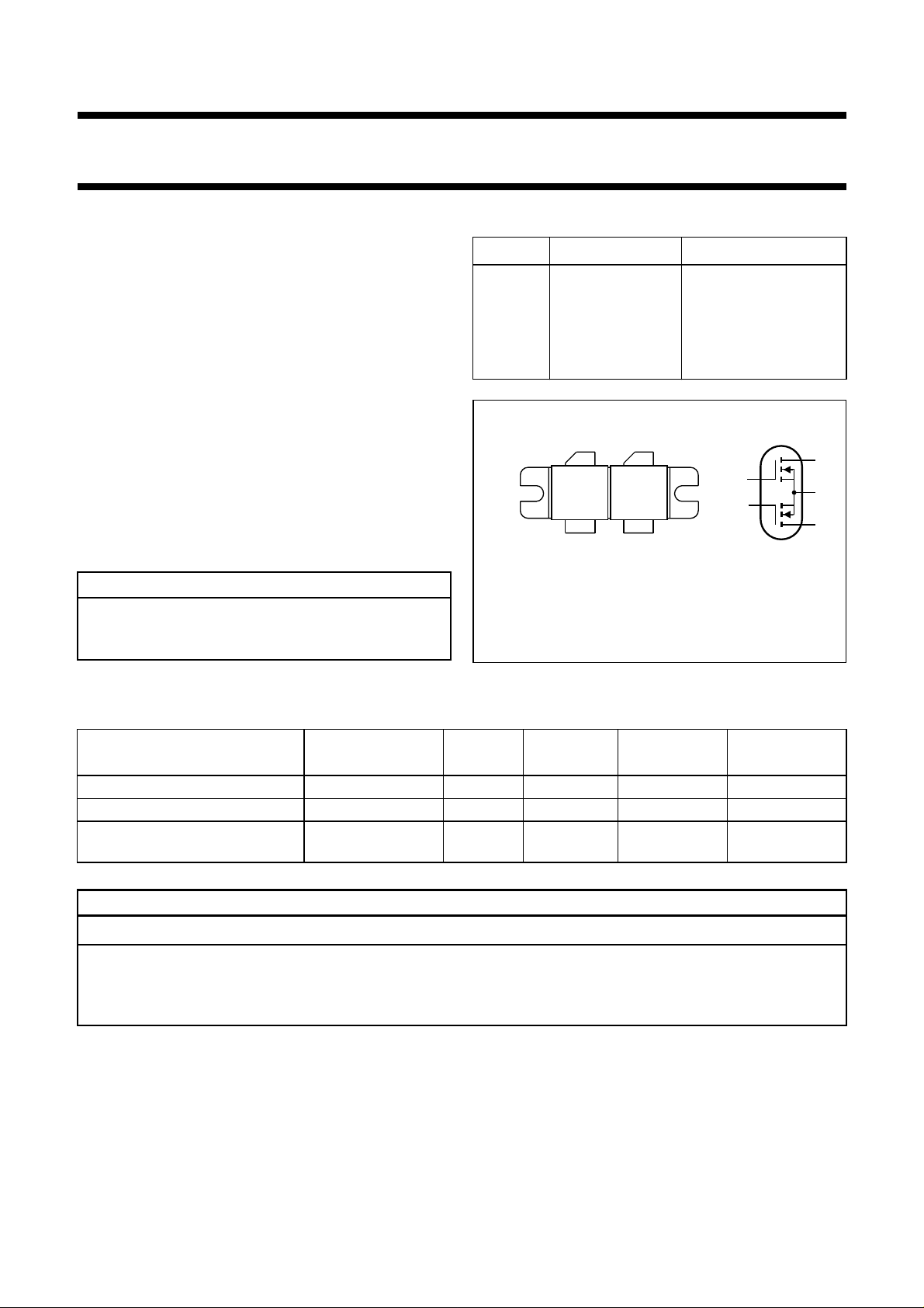
PINNING - SOT262A1
PIN SYMBOL DESCRIPTION
1d
2d
3g
4g
1
2
1
2
drain 1
drain 2
gate 1
gate 2
5 s source
12
g
g
55
Top view
34
MAM098
Fig.1 Simplified outline and symbol.
d
s
d
QUICK REFERENCE DATA
RF performance at T
MODE OF OPERATION
=25°C in a push-pull common source test circuit.
h
f
(MHz)
V
(V)
DS
P
(W)
L
G
p
(dB)
η
(%)
D
CW, class-B 108 50 300 >20 >60
CW, class-C 108 50 300 typ. 18 typ. 80
CW, class-AB 225 50 250 >14
typ. 16
>50
typ. 55
WARNING
Product and environmental safety - toxic materials
This product contains beryllium oxide. The product is entirely safe provided that the BeO discs are not damaged.
All persons who handle, use or dispose of this product should be aware of its nature and of the necessary safety
precautions. After use, dispose of as chemical or special waste according to the regulations applying at the location of
the user. It must never be thrown out with the general or domestic waste.
1996 Oct 21 2
Page 3
Philips Semiconductors Product Specification
VHF push-pull power MOS transistor BLF278
LIMITING VALUES
In accordance with the Absolute Maximum System (IEC 134).
SYMBOL PARAMETER CONDITIONS MIN. MAX. UNIT
Per transistor section
V
DS
V
GS
I
D
P
tot
T
stg
T
j
THERMAL CHARACTERISTICS
SYMBOL PARAMETER CONDITIONS VALUE UNIT
R
th j-mb
R
th mb-h
drain-source voltage − 110 V
gate-source voltage −±20 V
drain current (DC) − 18 A
total power dissipation up to Tmb=25°C total device;
− 500 W
both sections equally loaded
storage temperature −65 150 °C
junction temperature − 200 °C
thermal resistance from junction
to mounting base
thermal resistance from
mounting base to heatsink
total device; both sections
equally loaded.
total device; both sections
equally loaded.
max. 0.35 K/W
max. 0.15 K/W
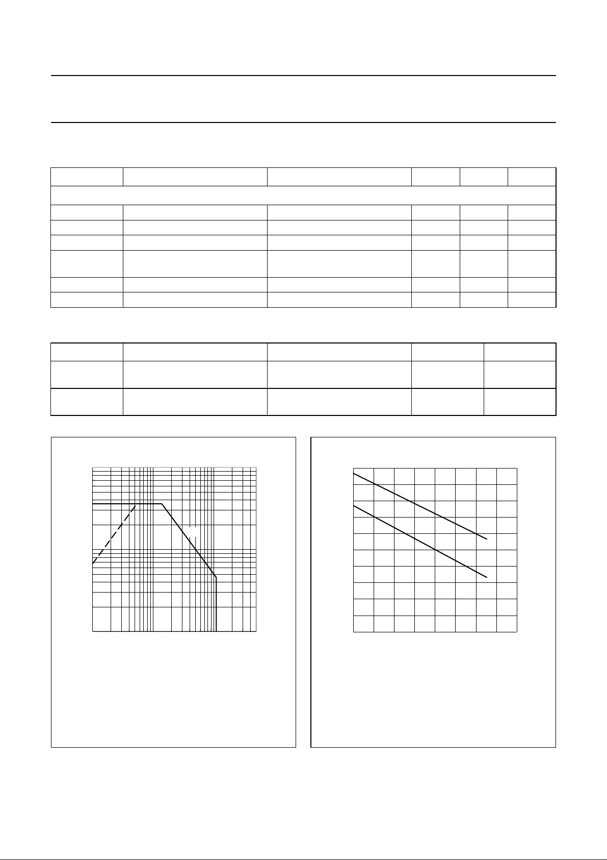
100
handbook, halfpage
I
D
(A)
(1)
10
1
1 10 100
Total device; both sections equally loaded.
(1) Current is this area may be limited by R
(2) Tmb=25°C.
Fig.2 DC SOAR.
(2)
DSon
MRA988
V (V)
DS
.
500
500
handbook, halfpage
P
tot
(W)
400
300
200
100
0
0 40 80 160
Total device; both sections equally loaded.
(1) Continuous operation.
(2) Short-time operation during mismatch.
(1)
Fig.3 Power derating curves.
(2)
120
MGE616
Th (°C)
1996 Oct 21 3
Page 4
Philips Semiconductors Product Specification
VHF push-pull power MOS transistor BLF278
CHARACTERISTICS
T
=25°C unless otherwise specified.
j
SYMBOL PARAMETER CONDITIONS MIN. TYP. MAX. UNIT
Per transistor section
V
(BR)DSS
I
DSS
I
GSS
V
GSth
∆V
GS
g
fs
g
fs1/gfs2
R
DSon
I
DSX
C
is
C
os
C
rs
C
d-f
drain-source breakdown voltage VGS= 0; ID=50mA 110 −−V
drain-source leakage current VGS= 0; VDS=50V −−2.5 mA
gate-source leakage current VGS= ±20 V; VDS=0 −−1µA
gate-source threshold voltage VDS=10V; ID=50mA 2 − 4.5 V
gate-source voltage difference
VDS=10V; ID=50mA −−100 mV
of both sections
forward transconductance VDS=10V; ID= 5 A 4.5 6.2 − S
forward transconductance ratio
VDS=10V; ID=5A 0.9 − 1.1
of both sections
drain-source on-state resistance VGS= 10 V; ID=5A − 0.2 0.3 Ω
drain cut-off current VGS= 10 V; VDS=10V − 25 − A
input capacitance VGS= 0; VDS= 50 V; f = 1 MHz − 480 − pF
output capacitance VGS= 0; VDS= 50 V; f = 1 MHz − 190 − pF
feedback capacitance VGS= 0; VDS= 50 V; f = 1 MHz − 14 − pF
drain-flange capacitance − 5.4 − pF
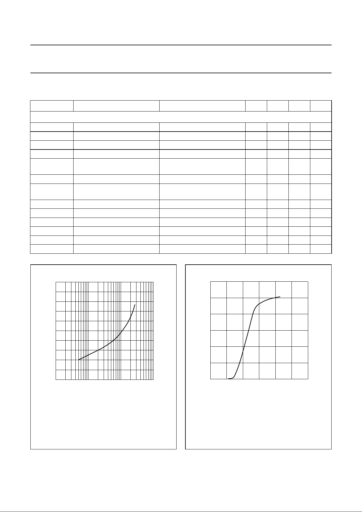
handbook, halfpage
0
T.C.
(mV/K)
−1
−2
−3
−4
−5
10
VDS=10V.
−2
−1
10
110
ID (A)
Fig.4 Temperature coefficient of gate-source
voltage as a function of drain current; typical
values per section.
MGE623
30
handbook, halfpage
I
D
(A)
20
10
0
0
VDS= 10V; Tj=25°C.
5
10
MGE622
VGS (V)
Fig.5 Drain current as a function of gate-source
voltage; typical values per section.
15
1996 Oct 21 4
Page 5
Philips Semiconductors Product Specification
VHF push-pull power MOS transistor BLF278
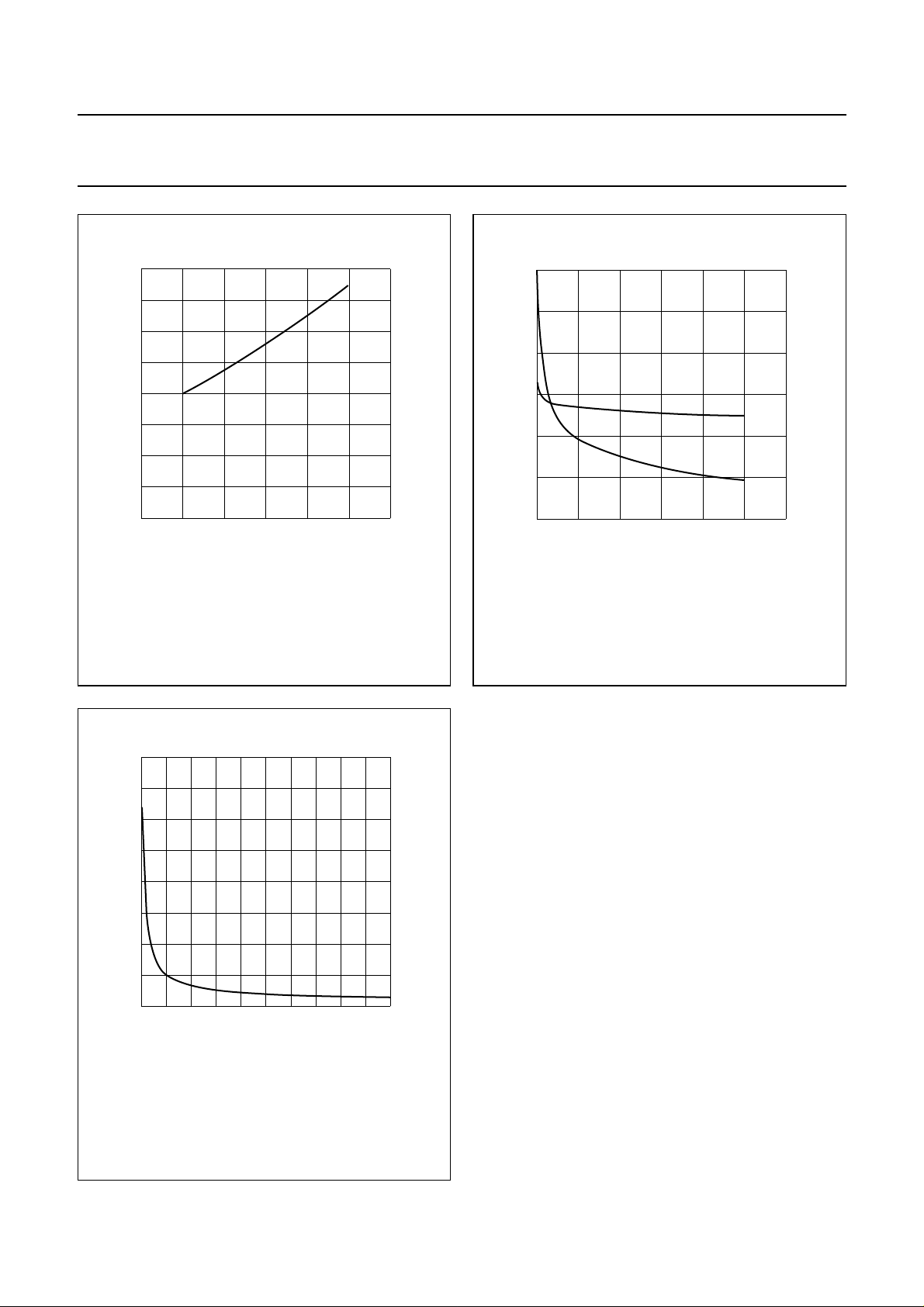
400
handbook, halfpage
R
DSon
(mΩ)
300
200
100
0
0 50 100 150
VGS= 10V; ID=5A.
Tj (°C)
Fig.6 Drain-source on-state resistance as a
function of junction temperature; typical
values per section.
MGE621
C
is
C
os
VDS (V)
MGE615
1200
handbook, halfpage
C
(pF)
800
400
0
0
VGS= 0; f= 1 MHz.
20
40
Fig.7 Input and output capacitance as functions
of drain-source voltage; typical values per
section.
60
400
handbook, halfpage
C
rs
(pF)
300
200
100
0
010 50
VGS= 0; f = 1 MHz.
20 30 40
VDS (V)
Fig.8 Feedback capacitance as a function of
drain-source voltage; typical values per
section.
MGE620
1996 Oct 21 5
Page 6
Philips Semiconductors Product Specification
VHF push-pull power MOS transistor BLF278
APPLICATION INFORMATION
Class-B operation
RF performance in CW operation in a common source push-pull test circuit. T
otherwise specified. R
=4Ω per section; optimum load impedance per section = 3.2 + j4.3 Ω (VDS= 50 V).
GS
=25°C; R
h
= 0.15 K/W unless
th mb-h
MODE OF OPERATION
f
(MHz)
V
(V)
DS
I
DQ
(A)
CW, class-B 108 50 2 × 0.1 300 >20
P
(W)
L
G
p
(dB)
η
(%)
D
>60
typ. 22
typ. 70
CW, class-C 108 50 VGS= 0 300 typ. 18 typ. 80
Ruggedness in class-B operation
The BLF278 is capable of withstanding a load mismatch corresponding to VSWR =7:1 through all phases under the
conditions: V
= 50 V; f = 108 MHz at rated load power.
DS
1996 Oct 21 6
Page 7
Philips Semiconductors Product Specification
VHF push-pull power MOS transistor BLF278
30
handbook, halfpage
G
p
(dB)
20
10
0
0
Class-B operation; VDS=50V;IDQ=2×0.1 A; f = 108 MHz;
= 3.2 + j4.3 Ω (per section); RGS=4Ω (per section).
Z
L
(1) Th=25°C.
(2) Th=70°C.
(1)
(2)
200 400 600
PL (W)
Fig.9 Power gain as a function of load power,
typical values.
MGE682
80
handbook, halfpage
η
D
(%)
60
(1)
40
20
0
0 200 400
Class-B operation; VDS=50V;IDQ=2×0.1 A; f = 108 MHz;
= 3.2 + j4.3 Ω (per section); RGS=4Ω (per section).
Z
L
(1) Th=25°C.
(2) Th=70°C.
(2)
(2)
(1)
PL (W)
Fig.10 Efficiency as a function of load power,
typical values.
MGE683
600
600
handbook, halfpage
P
L
(W)
400
200
0
0
Class-B operation; VDS=50V;IDQ=2×0.1 A; f = 108 MHz;
= 3.2 + j4.3 Ω (per section); RGS=4Ω (per section).
Z
L
(1) Th=25°C.
(2) Th=70°C.
(1)
(2)
51015
MGE684
Pi (W)
Fig.11 Load power as a function of input power,
typical values.
1996 Oct 21 7
Page 8

Philips Semiconductors Product Specification
VHF push-pull power MOS transistor BLF278
50 Ω
output
DD1
+V
C20
C16
C21
R2
C12
C8
L22
L21
C33
C31
L19L17L13
L11R8
C22
C13
R3
C9
A
C17
L12
R4
L9
D.U.T.
L3 L5 L7
L1
R10
C29 C30
C28
C27
C6 C7
C5
C34
C26
L4 L6 L8
L2
L23
C32
L14 L18 L20
L10
R5
MGE688
L15
C10
C23
C14
C18
C24
C25
DD2
+V
R7
C19
C11
C37
Fig.12 Class-B test circuit at f = 108 MHz.
R9 L16
C15
R6
C35
A
C3
R1
C2
C1
T1
50 Ω
input
handbook, full pagewidth
1996 Oct 21 8
C4
IC1
C36
R11
DD1
+V
Page 9

Philips Semiconductors Product Specification
VHF push-pull power MOS transistor BLF278
List of components (see Figs 12 and 13).
COMPONENT DESCRIPTION VALUE DIMENSIONS CATALOGUE NO.
C1, C2, C33, C34 multilayer ceramic chip capacitor;
note 1
C3, C4 multilayer ceramic chip capacitor;
note 1
C5, C6, C28 film dielectric trimmer 5 to 60 pF 2222 809 08003
C7 multilayer ceramic chip capacitor;
note 1
C8, C11, C12,
C15, C16, C19,
C36
C9, C10, C13,
C14, C20, C25
C17, C18, C22,
C23
C21, C24, C35 electrolytic capacitor 10 µF, 63 V
C26 multilayer ceramic chip capacitor;
C27 multilayer ceramic chip capacitor;
C29 multilayer ceramic chip capacitor;
C30 film dielectric trimmer 2 to 18 pF 2222 809 09006
C31, C32 multilayer ceramic chip capacitor;
L1, L2 stripline; note 2 43 Ω length 57.5 mm
L3, L4 stripline; note 2 43 Ω length 29.5 mm
L5, L6 stripline; note 2 43 Ω length 14 mm
L7, L8 stripline; note 2 43 Ω length 6 mm
L9, L10 stripline; note 2 43 Ω length 17.5 mm
L11, L16 2 × grade 3B Ferroxcube wideband
L12, L15 4 turns enamelled 2 mm copper wire 85 nH length 13.5 mm
L13, L14 stripline; note 2 43 Ω length 19.5 mm
multilayer ceramic chip capacitor 100 nF, 500 V 2222 852 47104
multilayer ceramic chip capacitor;
note 1
multilayer ceramic chip capacitor;
note 1
note 1
note 1
note 1
note 1
HF chokes in parallel
22 pF, 500 V
100 pF + 68 pF
in parallel, 500 V
2 × 100 pF +
1 × 120 pF in
parallel, 500 V
1 nF, 500 V
470 pF, 500 V
2 × 15 pF +
1 × 18 pF in
parallel, 500 V
3 × 15 pF in
parallel, 500 V
2 × 18 pF +
1 × 15 pF in
parallel, 500 V
3 × 43 pF in
parallel, 500 V
width 6 mm
width 6 mm
width 6 mm
width 6 mm
width 6 mm
4312 020 36642
int. dia. 10 mm
leads 2 × 7mm
width 6 mm
1996 Oct 21 9
Page 10

Philips Semiconductors Product Specification
VHF push-pull power MOS transistor BLF278
COMPONENT DESCRIPTION VALUE DIMENSIONS CATALOGUE NO.
L17, L18 stripline; note 2 43 Ω length 24.5 mm
width 6 mm
L19, L20 stripline; note 2 43 Ω length 66 mm
width 6 mm
L21, L23 stripline; note 2 50 Ω length 160 mm
width 4.8 mm
L22 semi-rigid cable; note 3 50 Ω ext. dia. 3.6 mm
outer conductor
length 160 mm
R1 metal film resistor 10 Ω, 0.4 W
R2, R7 10 turn potentiometer 50 kΩ
R3, R6 metal film resistor 3 × 12.1 Ω in
parallel, 0.4 W
R4, R5 metal film resistor 10 Ω; 0.4 W
R8, R9 metal film resistor 10 Ω±5%, 1 W
R10 metal film resistor 4 × 10 Ω in
parallel, 1 W
R11 metal film resistor 5.11 kΩ, 1W
IC1 voltage regulator 78L05
T1 1:1 Balun; 7 turns type 4C6 50 Ω
coaxial cable wound around toroid
14 × 9 × 5 mm 4322 020 90770
Notes
1. American Technical Ceramics capacitor, type 100B or capacitor of same quality.
2. L1 to L10, L13, L14, L17 to L21 and L23 are striplines on a double copper-clad printed-circuit board, with fibre-glass
PTFE dielectric (εr= 2.2), thickness1⁄16inch; thickness of copper sheet 2 × 35 µm.
3. L22 is soldered on to stripline L21.
1996 Oct 21 10
Page 11

Philips Semiconductors Product Specification
VHF push-pull power MOS transistor BLF278
handbook, full pagewidth
strap
strap
50 Ω
input
C3
R1
C2C1C4
C21
strap
strap
C28
150
L21
L19
L20
L23
L22
C29
C30
C31
C32
C34
MBC438
strap
strap
C33
R10
100
50 Ω
output
130
strap
strap
C20
V
DD1
T1
C5
R11
L1
L2
IC1
C36
slider R2
C6
slider R7
C8
C12
L3
L4
C15
C11
R2 and R7
C7
C35
C9
R3
R4
L5
L6L7L8
R5
R6
C10
C14
C13
L11
C22
C17
L9
L10
C18
C23 C24
C16
R8
L11
V
L12
L13
C26 C27
L14
L15
V
L16
R9
C19
L16
DD1
L17
L18
DD2
C25
Dimensions in mm.
The circuit and components are situated on one side of the PTFE fibre-glass board, the other side being fully metallized to serve as an earth.
Earth connections are made by means of copper straps for a direct contact between upper and lower sheets.
Fig.13 Printed-circuit board and component layout for 108 MHz class-B test circuit.
1996 Oct 21 11
Page 12

Philips Semiconductors Product Specification
VHF push-pull power MOS transistor BLF278
handbook, halfpage
2
Z
i
(Ω)
1
0
−1
−2
25 75 125
Class-B operation; VDS= 50 V; IDQ=2×0.1 A;
=4Ω (per section); PL= 300 W.
R
GS
r
i
x
i
MGE685
f (MHz)
Fig.14 Input impedance as a function of frequency
(series components), typical values per
section.
175
handbook, halfpage
8
Z
L
(Ω)
6
4
2
0
25 75 125
Class-B operation; VDS= 50 V; IDQ=2×0.1 A;
=4Ω (per section); PL= 300 W.
R
GS
R
L
X
L
MGE686
f (MHz)
Fig.15 Load impedance as a function of frequency
(series components), typical values per
section.
175
handbook, halfpage
Fig.16 Definition of MOS impedance.
30
handbook, halfpage
G
p
(dB)
20
10
Z
i
Z
MBA379
L
0
25
Class-B operation; VDS= 50 V; IDQ=2×0.1 A;
=4Ω (per section); PL= 300 W.
R
GS
75 125 175
MGE687
f (MHz)
Fig.17 Power gain as a function of frequency,
typical values per section.
1996 Oct 21 12
Page 13

Philips Semiconductors Product Specification
VHF push-pull power MOS transistor BLF278
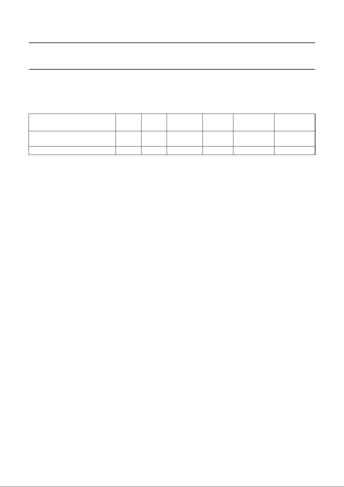
Class-AB operation
RF performance in CW operation in a common source push-pull test circuit. T
otherwise specified. R
= 2.8 Ω per section; optimum load impedance per section = 0.74 + j2 Ω; (VDS= 50 V).
GS
=25°C; R
h
= 0.15 K/W unless
th mb-h
MODE OF OPERATION
f
(MHz)
CW, class-AB 225 50 2 × 0.5 250 >14
V
(V)
DS
I
DQ
(A)
P
(W)
L
G
p
(dB)
η
(%)
D
>50
typ. 16
typ. 55
Ruggedness in class-AB operation
The BLF278 is capable of withstanding a load mismatch corresponding to VSWR =7:1 through all phases under the
conditions: V
= 50 V; f = 225 MHz at rated output power.
DS
1996 Oct 21 13
Page 14

Philips Semiconductors Product Specification
VHF push-pull power MOS transistor BLF278
20
handbook, halfpage
G
p
(dB)
10
0
0 100 200 300
Class-AB operation; VDS= 50 V; IDQ=2×0.5 A; f = 225 MHz;
= 0.74 + j2 Ω (per section); RGS= 2.8 Ω (per section).
Z
L
(1) Th=25°C.
(2) Th=70°C.
(1)
(2)
PL (W)
Fig.18 Power gain as a function of load power,
typical values.
MGE614
60
handbook, halfpage
η
D
(%)
40
20
0
0
Class-AB operation; VDS= 50 V; IDQ=2×0.5 A; f = 225 MHz;
= 0.74 + j2 Ω (per section); RGS= 2.8 Ω (per section).
Z
L
(1) Th=25°C.
(2) Th=70°C.
(1)
(2)
100 200
PL (W)
Fig.19 Efficiency as a function of load power,
typical values.
MGE612
300
400
handbook, halfpage
P
L
(W)
300
(1)
200
100
0
0 5 10 15
Class-AB operation; VDS= 50 V; IDQ=2×0.5 A; f = 225 MHz;
= 0.74 + j2 Ω (per section); RGS= 2.8 Ω (per section).
Z
L
(1) Th=25°C.
(2) Th=70°C.
(2)
MGE613
Pi (W)
Fig.20 Load power as a function of input power,
typical values.
1996 Oct 21 14
Page 15

Philips Semiconductors Product Specification
VHF push-pull power MOS transistor BLF278
50 Ω
output
C22
DD1
+V
handbook, full pagewidth
C14
C23
R2
L14R8
C10
A
C15
R3
C24
C11
C8
C16
L15
R4
L23
L22
C33
C31
L20L18L12
D.U.T.
L6 L8 L10
L4
R10
C34
C21 C28 C29 C30
C20
C6 C7
C5
L7 L9 L11
L5L3
L24
C32
L19 L21
L13
MGE617
R5
L16
C17
C9
C25
C12
C18
A
R6
C13
C35
L17
R9
R7
C26
C36
C37
C27
DD2
+V
C19
Fig.21 Class-AB test circuit at f = 225 MHz.
C1
R1
C4
C2
L2
50 Ω
input
C3
L1
1996 Oct 21 15
IC1
C38
R11
DD1
+V
Page 16

Philips Semiconductors Product Specification
VHF push-pull power MOS transistor BLF278
List of components (see Figs 21 and 22).
COMPONENT DESCRIPTION VALUE DIMENSIONS CATALOGUE NO.
C1, C2 multilayer ceramic chip capacitor;
note 1
C3, C4, C31, C32 multilayer ceramic chip capacitor;
note 1
C5 film dielectric trimmer 4 to 40 pF 2222 809 08002
C6, C30 film dielectric trimmer 2 to 18 pF 2222 809 09006
C7 multilayer ceramic chip capacitor;
note 1
C8, C9, C15, C18 MKT film capacitor 1 µF, 63 V 2222 371 11105
C10, C13, C14,
C19, C36
C11, C12 multilayer ceramic chip capacitor;
C16, C17 electrolytic capacitor 220 µF, 63 V
C20 multilayer ceramic chip capacitor;
C21 film dielectric trimmer 2 to 9 pF 2222 809 09005
C22, C27, C37,
C38
C23, C26, C35 electrolytic capacitor 10 µF, 63 V
C24, C25 multilayer ceramic chip capacitor;
C28 multilayer ceramic chip capacitor;
C29 multilayer ceramic chip capacitor;
C33, C34 multilayer ceramic chip capacitor;
L1, L3, L22, L24 stripline; note 2 50 Ω length 80 mm
L2, L23 semi-rigid cable; note 3 50 Ω ext. dia. 3.6 mm
L4, L5 stripline; note 2 43 Ω length 24 mm
L6, L7 stripline; note 2 43 Ω length 14.5 mm
L8, L9 stripline; note 2 43 Ω length 4.4 mm
L10, L11 stripline; note 2 43 Ω length 3.2 mm
L12, L13 stripline; note 2 43 Ω length 15 mm
multilayer ceramic chip capacitor 100 nF, 50 V 2222 852 47104
note 1
note 1
multilayer ceramic chip capacitor;
note 1
note 1
note 1
note 1
note 1
27 pF, 500 V
3 × 18 pF
in parallel, 500 V
100 pF, 500 V
2 × 1 nF in parallel,
500 V
3 × 33 pF in
parallel, 500 V
1 nF, 500 V
2 × 470 pF in
parallel, 500 V
2 × 10 pF +
1 × 18 pF in
parallel, 500 V
2 × 5.6 pF in
parallel, 500 V
5.6 pF, 500 V
width 4.8 mm
outer conductor
length 80 mm
width 6 mm
width 6 mm
width 6 mm
width 6 mm
width 6 mm
1996 Oct 21 16
Page 17

Philips Semiconductors Product Specification
VHF push-pull power MOS transistor BLF278
COMPONENT DESCRIPTION VALUE DIMENSIONS CATALOGUE NO.
L14, L17 2 × grade 3B Ferroxcube
wideband HF chokes in parallel
L15, L16 1
L18, L19 stripline; note 2 43 Ω length 13 mm
L20, L21 stripline; note 2 43 Ω length 29.5 mm
R1 metal film resistor 10 Ω, 0.4 W
R2, R7 10 turns potentiometer 50 kΩ
R3, R6 metal film resistor 1 kΩ, 0.4 W
R4, R5 metal film resistor 2 × 5.62 Ω, in
R8, R9 metal film resistor 10 Ω±5%, 1 W
R10 metal film resistor 4 × 42.2 Ω in
R11 metal film resistor 5.11 kΩ, 1W
IC1 voltage regulator 78L05
3
⁄4turns enamelled 2 mm copper
wire
40 nH int. dia. 10 mm
leads 2 × 7mm
space 1 mm
width 6 mm
width 6 mm
parallel, 0.4 W
parallel, 1 W
4312 020 36642
Notes
1. American Technical Ceramics capacitor, type 100B or other capacitor of the same quality.
2. L1, L3 to L13, L18 to L22 and L24 are microstriplines on a double copper-clad printed-circuit board, with fibre-glass
reinforced PTFE dielectric (εr= 2.2), thickness1⁄16inch; thickness of copper sheet 2 × 35 µm.
3. L2 and L23 are soldered on to striplines L1 and L24 respectively.
1996 Oct 21 17
Page 18

Philips Semiconductors Product Specification
VHF push-pull power MOS transistor BLF278
handbook, full pagewidth
strap
strap
L1
50 Ω
input
V
DD1
Hollow
rivets
R1
C30
C23
C32
C26
C31
130
C33
L23
C34
R10
L22
L24
Hollow
rivets
strap
strap
MBC436
100
50 Ω
output
119
C15
C18
strap
strap
C24
C14
L14
R8
L14
L15
L18
C28
C21
L19
L16
L17
R9
L17
C25 C27
C19
V
L20
L21
V
C22
DD1
C29
DD2
strap
strap
to R2,R7
C38
slider R2
C3
C4
slider R7
IC1
C35
C5
L4
L5
C10
C13
C36
C6
C37
C11
R6
C12
R3
R4
L7 L9
R5
C16
L8L6
C17
C9
C8
C7
L10
L11
L12
C20
L13
R11
L2
C1
C2
L3
Dimensions in mm.
The circuit and components are situated on one side of the PTFE fibre-glass board, the other side being fully metallized to serve as an earth.
Earth connections are made by means of copper straps for a direct contact between upper and lower sheets.
Fig.22 Printed-circuit board and component layout for 225 MHz class-AB test circuit.
1996 Oct 21 18
Page 19

Philips Semiconductors Product Specification
VHF push-pull power MOS transistor BLF278
handbook, halfpage
2
z
i
(Ω)
1
0
−1
–2
150 200 250
Class-AB operation; VDS= 50 V; IDQ=2×0.5 A;
= 2.8 Ω (per section); PL= 250 W.
R
GS
r
i
x
i
f (MHz)
MGE611
Fig.23 Input impedance as a function of frequency
(series components), typical values per
section.
handbook, halfpage
3
X
Z
L
(Ω)
2
1
0
150 250200
Class-AB operation; VDS= 50 V; IDQ=2×0.5 A;
= 2.8 Ω (per section); PL= 250 W.
R
GS
L
R
L
f (MHz)
MGE625
Fig.24 Load impedance as a function of frequency
(series components), typical values per
section.
handbook, halfpage
Fig.25 Definition of MOS impedance.
20
handbook, halfpage
G
p
(dB)
10
Z
i
Z
MBA379
L
0
150 200 250
Class-AB operation; VDS= 50 V; IDQ=2×0.5 A;
= 2.8 Ω (per section); PL= 250 W.
R
GS
f (MHz)
MGE624
Fig.26 Power gain as a function of frequency,
typical values per section.
1996 Oct 21 19
Page 20

Philips Semiconductors Product Specification
VHF push-pull power MOS transistor BLF278
PACKAGE OUTLINE
0.25
Dimensions in mm.
2.92
2.29
1.02
0.13
2.54
10.4
max
21.85
11.05
27.94
34.3 max
11 max
5.9
5.5
(4x)
43
11 max
12
5.525
seating plane
0.25 M
5
1.65
3.3
3.0
5.8
max
9.8
MSA285 - 2
15.6
max
Fig.27 SOT262A1.
1996 Oct 21 20
Page 21

Philips Semiconductors Product Specification
VHF push-pull power MOS transistor BLF278
DEFINITIONS
Data Sheet Status
Objective specification This data sheet contains target or goal specifications for product development.
Preliminary specification This data sheet contains preliminary data; supplementary data may be published later.
Product specification This data sheet contains final product specifications.
Limiting values
Limiting values given are in accordance with the Absolute Maximum Rating System (IEC 134). Stress above one or
more of the limiting values may cause permanent damage to the device. These are stress ratings only and operation
of the device at these or at any other conditions above those given in the Characteristics sections of the specification
is not implied. Exposure to limiting values for extended periods may affect device reliability.
Application information
Where application information is given, it is advisory and does not form part of the specification.
LIFE SUPPORT APPLICATIONS
These products are not designed for use in life support appliances, devices, or systems where malfunction of these
products can reasonably be expected to result in personal injury. Philips customers using or selling these products for
use in such applications do so at their own risk and agree to fully indemnify Philips for any damages resulting from such
improper use or sale.
1996 Oct 21 21
 Loading...