

Page 1
DISCRETE SEMICONDUCTORS
DATA SH EET
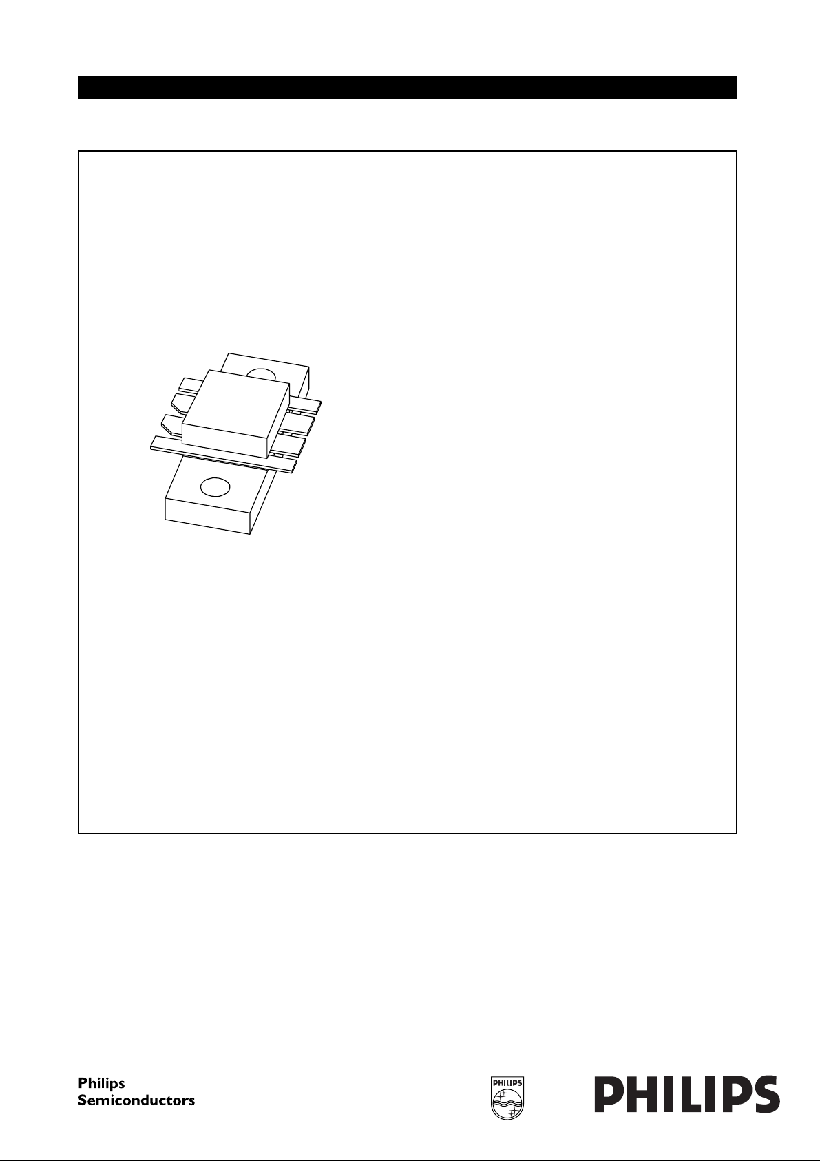
dbook, halfpage
M3D075
BLF246B
VHF push-pull power MOS
transistor
Product specification
Supersedes data of October 1992
1999 Jan 28
Page 2
Philips Semiconductors Product specification
VHF push-pull power MOS transistor BLF246B
FEATURES
• High power gain
• Easy power control
• Good thermal stability
• Gold metallization ensures
excellent reliability.
APPLICATIONS
Large signal applications in the VHF
frequency range.
DESCRIPTION
Silicon N-channel enhancement
mode vertical D-MOS push-pull
transistor encapsulated in an 8-lead
SOT161A balanced flange package
with a ceramic cap. All leads are
isolated from the flange.
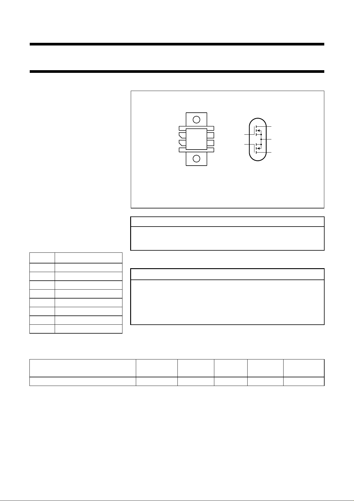
PINNING - SOT161A
PIN CONFIGURATION
ndbook, halfpage
d
MBB157
2
s
d
1
1
3
5
78
Top view
2
4
6
MBC826
g
2
g
1
Fig.1 Simplified outline and symbol.
CAUTION
This product is supplied in anti-static packing to prevent damage caused by
electrostatic discharge during transport and handling. For further information,
refer to Philips specs.: SNW-EQ-608, SNW-FQ-302A, and SNW-FQ-302B.
PIN DESCRIPTION
1 source
2 source
3 drain 1
4 gate 1
5 drain 2
6 gate 2
7 source
Product and environmental safety - toxic materials
This product contains beryllium oxide. The product is entirely safe provided
that the BeO disc is not damaged. All persons who handle, use or dispose of
this product should be aware of its nature and of the necessary safety
precautions. After use, dispose of as chemical or special waste according to
the regulations applying at the location of the user. It must never be thrown
out with the general or domestic waste.
WARNING
8 source
QUICK REFERENCE DATA
RF performance at T
MODE OF OPERATION
=25°C in a push-pull common source test circuit.
h
f
(MHz)
V
(V)
DS
P
(W)
L
G
(dB)
p
(%)
CW, class-AB 175 28 60 >14 >55
η
D
1999 Jan 28 2
Page 3
Philips Semiconductors Product specification
VHF push-pull power MOS transistor BLF246B
LIMITING VALUES
In accordance with the Absolute Maximum Rating System (IEC 134).
SYMBOL PARAMETER CONDITIONS MIN. MAX. UNIT
Per transistor section unless otherwise specified
V
DS
V
GS
I
D
P
tot
T
stg
T
j
THERMAL CHARACTERISTICS
SYMBOL PARAMETER CONDITIONS VALUE UNIT
R
th j-mb
R
th mb-h
drain-source voltage − 65 V
gate-source voltage −±20 V
drain current (DC) − 8A
total power dissipation Tmb≤ 25 °C total device; both sections equally loaded − 130 W
storage temperature −65 +150 °C
junction temperature − 200 °C
thermal resistance from junction to
mounting base
thermal resistance from mounting base
to heatsink
total device; both sections equally
loaded
total device; both sections equally
loaded
1.35 K/W
0.25 K/W
50
handbook, halfpage
I
D
(A)
10
(1)
1
−1
10
110
(1) Current in this area may be limited by R
(2) Tmb=25°C.
Total device; both sections equally loaded.
Fig.2 DC SOAR.
(2)
VDS (V)
DSon
120
MGR738
Th (°C)
MRA932
2
10
.
160
handbook, halfpage
P
tot
(W)
120
80
40
0
0 40 80 160
(1) Continuous operation.
(2) Short-time operation during mismatch.
Total device; both sections equally loaded.
(2)
(1)
Fig.3 Power/temperature derating curves.
1999 Jan 28 3
Page 4
Philips Semiconductors Product specification
VHF push-pull power MOS transistor BLF246B
CHARACTERISTICS
T
=25°C unless otherwise specified.
j
SYMBOL PARAMETER CONDITIONS MIN. TYP. MAX. UNIT
Per transistor section
V
(BR)DSS
I
DSS
I
GSS
V
GSth
g
fs
R
DSon
I
DSX
C
is
C
os
C
rs
drain-source breakdown voltage VGS= 0; ID=10mA 65 −−V
drain-source leakage current VGS= 0; VDS=28V −−2mA
gate-source leakage current VGS= ±20 V; VDS=0 −−1µA
gate-source threshold voltage ID= 10 mA; VDS=10V 2 − 4.5 V
forward transconductance ID= 1.5 A; VDS= 10 V 1.2 1.8 − S
drain-source on-state resistance ID= 1.5 A; VGS=10V − 0.4 0.75 Ω
on-state drain current VGS= 10 V; VDS=10V − 10 − A
input capacitance VGS= 0; VDS=28V; f=1MHz − 125 − pF
output capacitance VGS= 0; VDS=28V; f=1MHz − 75 − pF
feedback capacitance VGS= 0; VDS=28V; f=1MHz − 11 − pF
handbook, halfpage
6
T.C.
(mV/K)
4
2
0
−2
−4
−6
10 10
VDS=10V.
2
3
10
ID (mA)
Fig.4 Temperature coefficient of gate-source
voltage as a function of drain current; typical
values per section.
MGR739
12
handbook, halfpage
I
D
(A)
8
4
4
10
0
020
VDS=10V.
10
Tj = 25 °C
125 °C
VGS (V)
MGR740
Fig.5 Drain current as a function of gate-source
voltage; typical values per section.
1999 Jan 28 4
Page 5
Philips Semiconductors Product specification
VHF push-pull power MOS transistor BLF246B
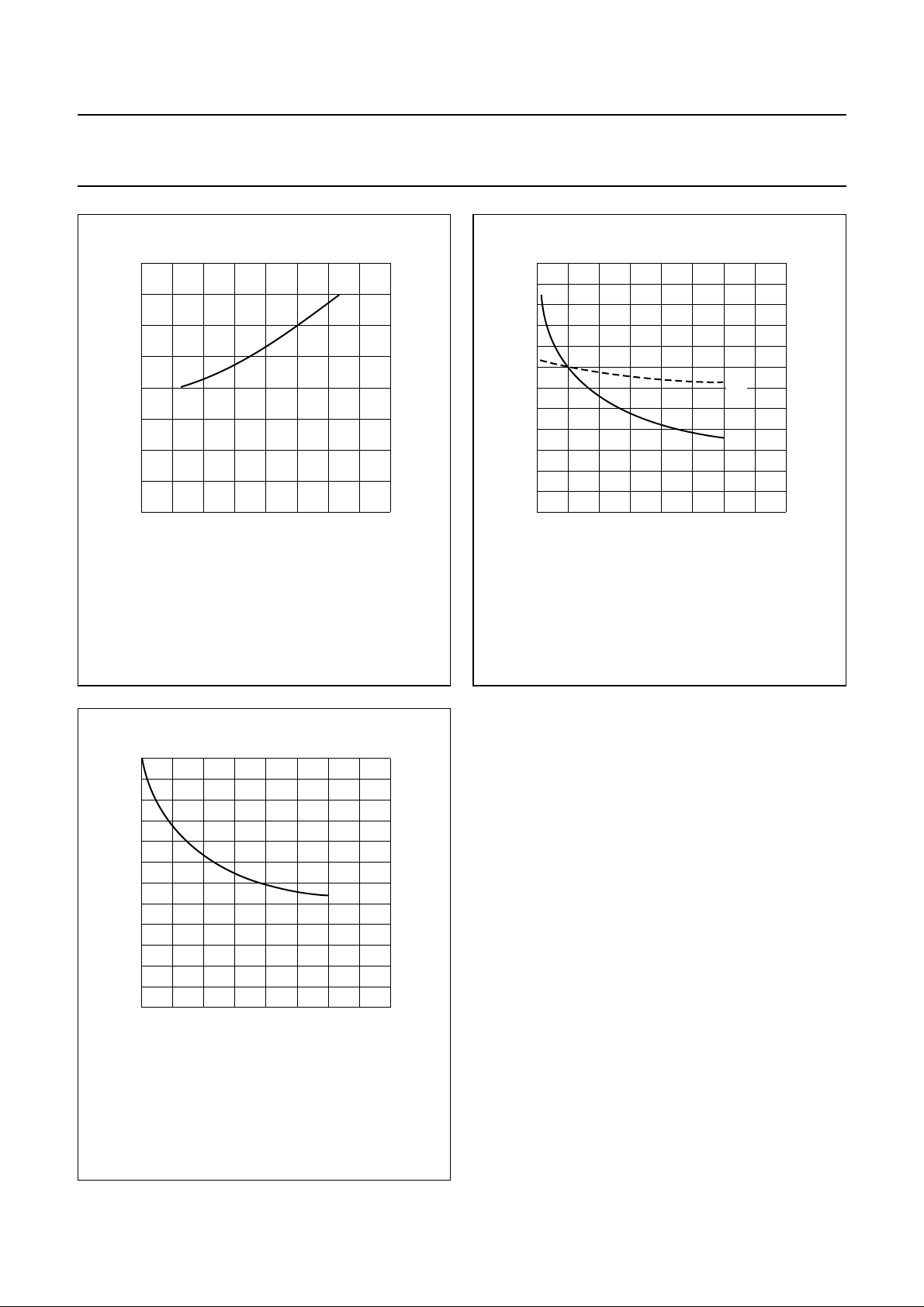
0.8
handbook, halfpage
R
DSon
(Ω)
0.6
0.4
0.2
0
0 40 80 160
VGS= 10V; ID= 1.5 A.
120
Fig.6 Drain-source on-state resistance as a
function of junction temperature; typical
values per section.
MGR741
Tj (°C)
30
C
is
C
os
VDS (V)
MGR742
240
handbook, halfpage
C
(pF)
180
120
60
0
01020 40
VGS= 0; f = 1 MHz.
Fig.7 Input and output capacitance as functions
of drain-source voltage; typical values per
section.
24
handbook, halfpage
C
rs
(pF)
18
12
6
0
01020 40
VGS= 0; f = 1 MHz.
30
VDS (V)
Fig.8 Feedback capacitance as a function of
drain-source voltage; typical values per
section.
MGR743
1999 Jan 28 5
Page 6

Philips Semiconductors Product specification
VHF push-pull power MOS transistor BLF246B
APPLICATION INFORMATION
RF performance in CW operation in a push-pull, common source, class-B circuit. T
unless otherwise specified.
=25°C; R
h
th mb-h
= 0.25 K/W;
MODE OF OPERATION
f
(MHz)
V
(V)
DS
I
DQ
(mA)
P
(W)
L
G
p
(dB)
η
(%)
D
CW, class-B 175 28 2 × 50 60 >14 >55
typ. 19 typ. 65
Ruggedness in class-B operation
The BLF246B is capable of withstanding a load mismatch corresponding to VSWR = 50 : 1 through all phases under the
following conditions: V
25
handbook, halfpage
G
p
(dB)
20
15
10
5
= 28 V; f = 175 MHz at rated output power.
DS
MGR744
100
η
D
G
p
η
D
(%)
80
60
40
20
100
handbook, halfpage
P
L
(W)
80
60
40
20
MGR745
0
02040 80
Class-B operation; VDS= 28 V; IDQ=2×50 mA;
= 4.6 + j5 Ω; f = 175 MHz.
Z
L
60
PL (W)
0
Fig.9 Power gain and efficiency as a function of
load power; typical values per section.
1999 Jan 28 6
0
Class-B operation; VDS= 28 V; IDQ=2×50 mA;
= 4.6 + j5 Ω; f = 175 MHz.
Z
L
0.5 1.0 1.5 2.0
0 2.5
PIN (W)
Fig.10 Load power as a function of input power;
typical values per section.
Page 7

Philips Semiconductors Product specification
VHF push-pull power MOS transistor BLF246B
handbook, full pagewidth
50 Ω
input
+V
L12
D
C11
C12
C13
C14
C15
L13
L10
L16
C21 C22 C23 C24
L11
L17
L14
C16
C17
R7
L18
L19
R8
L20
L21
C25
C26
L22
L23
L24
50 Ω
output
+V
R1
R2
R5
G
C7
C8
C6C4 C5
R3
C1
L1
L2
C2
L3
C3
L4
L5
L6L7L8
L9
C10
C9
+V
G
R4
f = 175 MHz.
Fig.11 Test circuit for class-B operation.
1999 Jan 28 7
R6
L15
+V
C18
C19
C20
MGR749
D
Page 8

Philips Semiconductors Product specification
VHF push-pull power MOS transistor BLF246B
List of components class-B test circuit (see Figs 11 and 12)
COMPONENT DESCRIPTION VALUE DIMENSIONS CATALOGUE No.
C1, C2, C25, C26 multilayer ceramic chip capacitor
(note 1)
C3 film dielectric trimmer 4 to 40 pF 2222 809 08002
C4 multilayer ceramic chip capacitor
(note 1)
C5, C22, C24 film dielectric trimmer 5 to 60 pF 2222 809 08003
C6 multilayer ceramic chip capacitor
(note 1)
C7, C9, C12, C14,
C17, C19
multilayer ceramic chip capacitor
(note 1)
C8, C10, C15, C16 multilayer ceramic chip capacitor
(note 1)
C11, C20 multilayer ceramic chip capacitor
(note 1)
C13, C18 electrolytic capacitor 10 µF, 63 V
C21 multilayer ceramic chip capacitor
(note 1)
C23 multilayer ceramic chip capacitor
(note 1)
L1, L3, L22, L24 stripline (note 2) 55 Ω 111 × 2.5 mm
L2, L23 semi-rigid cable 50 Ω length 111 mm
L4, L5 stripline (note 2) 50 Ω 6.5 × 2.8 mm
L6, L7 stripline (note 2) 50 Ω 35 × 2.8 mm
L8, L9 stripline (note 2) 50 Ω 5 × 2.8 mm
L10, L11 stripline (note 2) 50 Ω 9 × 2.8 mm
L12, L15 grade 3B Ferroxcube wideband
HF choke
L13, L14 4 turns enamelled 1 mm copper wire 50 nH length 6.5 mm
L16, L17 stripline (note 2) 50Ω 17 × 2.8 mm
L18, L19 stripline (note 2) 50Ω 26 × 2.8 mm
L20, L21 stripline (note 2) 50Ω 4 × 2.8 mm
R1, R2, R7, R8 metal film resistor 0.4 W, 10 Ω
R3, R4 10 turns potentiometer 50 kΩ
R5, R6 metal film resistor 0.4 W, 205 kΩ
91 pF
180 pF
100 pF
100 nF 2222 852 47104
680 PF
10 nF 2222 852 47103
82 pF
33 pF
ext. dia 2.2 mm
4312 020 36642
int. dia. 4 mm
leads 2 × 5mm
Notes
1. American Technical Ceramics (ATC) capacitor, type 100B or other capacitor of the same quality.
2. The striplines are on a double copper-clad printed circuit board with epoxy glass dielectric (ε
1
⁄16inch. The other side of the board is fully metallized and used as a ground plane. The ground planes on each side
= 4.5); thickness
r
of the board are connected together by means of copper straps and hollow rivets.
1999 Jan 28 8
Page 9

Philips Semiconductors Product specification
VHF push-pull power MOS transistor BLF246B
handbook, full pagewidth
110
strap
strap
rivet
L1 + L2
C1
C2
C3
200
R7
+V
D
C12
L18
L19
rivet
C13
rivet
C23
C24
strap
rivet
strap
L22
L20
C25
C26
L21
rivet
strapstrap
strap strap
rivet
+V
G
L12
C11
C14
C6
L8
L9
L10
L11
C15
C16
L16
L17
L13
L14
C21
C22
C7
C8
R1
C4
C5
R2
C10
C9
L6
L7
L4
L5
L15
C19
R3
+V
C20
C18
D
C17
L3
+V
G
Dimensions in mm.
The circuit and components are situated on one side of the PTFE fibre-glass board, the other side being fully metallized, to serve as a ground plane.
Earth connections are made by means of copper straps and hollow rivets for a direct contact between upper and lower sheets.
L23 + L24
MGR750
Fig.12 Component layout for 175 MHz class-B test circuit.
1999 Jan 28 9
Page 10

Philips Semiconductors Product specification
VHF push-pull power MOS transistor BLF246B
300
MGR746
f (MHz)
10
handbook, halfpage
Z
i
(Ω)
r
5
0
−5
Class-B operation; VDS= 28 V; IDQ=2×50 mA;
=10Ω; PL= 60 W (total device).
R
GS
i
x
i
0 100 200 400
Fig.13 Input impedance as a function of frequency
(series components); typical values per
section.
300
MGR747
f (MHz)
15
handbook, halfpage
Z
L
(Ω)
10
5
0
Class-B operation; VDS= 28 V; IDQ=2×50 mA;
=10Ω; PL= 60 W (total device).
R
GS
R
L
X
L
0 100 200 400
Fig.14 Load impedance as a function of frequency
(series components); typical values per
section.
handbook, halfpage
Fig.15 Definition of MOS impedance.
3000
MGR748
f (MHz)
25
handbook, halfpage
G
p
(dB)
20
15
Z
i
Z
MBA379
L
10
5
0
Class-B operation; VDS= 28 V; IDQ=2×50 mA;
=10Ω; PL= 60 W (total device).
R
GS
100 200 400
Fig.16 Power gain as a function of frequency;
typical values per section.
1999 Jan 28 10
Page 11

Philips Semiconductors Product specification
VHF push-pull power MOS transistor BLF246B
PACKAGE OUTLINE
Flanged ceramic package; 2 mounting holes; 8 leads SOT161A
D
A
F
U
1
q
scale
w
2
p
w
3
H
1
b
1
5
H
U
2
A
876
e
1
1
3
4
2
b
e
0 5 10 mm
M
M
C
B
C
c
E
w
M
AB
1
Q
DIMENSIONS (millimetre dimensions are derived from the original inch dimensions)
UNIT
inches
A
2.04
7.27
mm
OUTLINE
VERSION
SOT161A 97-06-28
6.47
0.286
0.255
1.77
0.080
0.070
c
b
1
2.93
2.66
0.115
0.105
Db
E
e
e
1
10.22
10.00
0.402
0.394
10.22
10.00
0.402
0.394
3.80
3.50
0.138
0.150
REFERENCES
0.18
0.10
0.007
0.004
IEC JEDEC EIAJ
F
2.70
2.08
0.106
0.082
H
17.00
16.00
0.669
0.630
H
1
12.83
12.57
0.505
0.495
3.36
2.92
0.132
0.120
qw
18.42
U
U
1
10.34
24.97
10.08
24.71
0.407
0.983
0.397
0.973
EUROPEAN
PROJECTION
2
p
Q
4.32
4.06
0.170
0.160
1999 Jan 28 11
w
1
w
3
2
0.260.51 1.02
0.010.02 0.040.725
ISSUE DATE
Page 12

Philips Semiconductors Product specification
VHF push-pull power MOS transistor BLF246B
DEFINITIONS
Data Sheet Status
Objective specification This data sheet contains target or goal specifications for product development.
Preliminary specification This data sheet contains preliminary data; supplementary data may be published later.
Product specification This data sheet contains final product specifications.
Limiting values
Limiting values given are in accordance with the Absolute Maximum Rating System (IEC 134). Stress above one or
more of the limiting values may cause permanent damage to the device. These are stress ratings only and operation
of the device at these or at any other conditions above those given in the Characteristics sections of the specification
is not implied. Exposure to limiting values for extended periods may affect device reliability.
Application information
Where application information is given, it is advisory and does not form part of the specification.
LIFE SUPPORT APPLICATIONS
These products are not designed for use in life support appliances, devices, or systems where malfunction of these
products can reasonably be expected to result in personal injury. Philips customers using or selling these products for
use in such applications do so at their own risk and agree to fully indemnify Philips for any damages resulting from such
improper use or sale.
1999 Jan 28 12
Page 13

Philips Semiconductors Product specification
VHF push-pull power MOS transistor BLF246B
NOTES
1999 Jan 28 13
Page 14

Philips Semiconductors Product specification
VHF push-pull power MOS transistor BLF246B
NOTES
1999 Jan 28 14
Page 15

Philips Semiconductors Product specification
VHF push-pull power MOS transistor BLF246B
NOTES
1999 Jan 28 15
Page 16

Philips Semiconductors – a worldwide company
Argentina: see South America
Australia: 34 Waterloo Road, NORTH RYDE, NSW 2113,
Tel. +61 2 9805 4455, Fax. +61 2 9805 4466
Austria: Computerstr. 6, A-1101 WIEN, P.O. Box 213,
Tel. +43 1 60 101 1248, Fax. +43 1 60 101 1210
Belarus: Hotel Minsk Business Center, Bld. 3, r. 1211, Volodarski Str. 6,
220050 MINSK, Tel. +375 172 20 0733, Fax. +375 172 20 0773
Belgium: see The Netherlands
Brazil: seeSouth America
Bulgaria: Philips Bulgaria Ltd., Energoproject, 15thfloor,
51 James Bourchier Blvd., 1407 SOFIA,
Tel. +359 2 68 9211, Fax. +359 2 68 9102
Canada: PHILIPS SEMICONDUCTORS/COMPONENTS,
Tel. +1 800 234 7381, Fax. +1 800 943 0087
China/Hong Kong: 501 Hong Kong Industrial Technology Centre,
72 Tat Chee Avenue, Kowloon Tong, HONG KONG,
Tel. +852 2319 7888, Fax. +852 2319 7700
Colombia: see South America
Czech Republic: see Austria
Denmark: Sydhavnsgade 23, 1780 COPENHAGEN V,
Tel. +45 33 29 3333, Fax. +45 33 29 3905
Finland: Sinikalliontie 3, FIN-02630 ESPOO,
Tel. +358 9 615 800, Fax. +358 9 6158 0920
France: 51 Rue Carnot, BP317, 92156 SURESNES Cedex,
Tel. +33 1 4099 6161, Fax. +33 1 4099 6427
Germany: Hammerbrookstraße 69, D-20097 HAMBURG,
Tel. +49 40 2353 60, Fax. +49 40 2353 6300
Greece: No. 15, 25th March Street, GR 17778 TAVROS/ATHENS,
Tel. +30 1 489 4339/4239, Fax. +30 1 481 4240
Hungary: seeAustria
India: Philips INDIA Ltd, Band Box Building, 2nd floor,
254-D, Dr. Annie Besant Road, Worli, MUMBAI 400 025,
Tel. +91 22 493 8541, Fax. +91 22 493 0966
Indonesia: PT Philips Development Corporation, Semiconductors Division,
Gedung Philips, Jl. Buncit Raya Kav.99-100, JAKARTA 12510,
Tel. +62 21 794 0040 ext. 2501, Fax. +62 21 794 0080
Ireland: Newstead, Clonskeagh, DUBLIN 14,
Tel. +353 1 7640 000, Fax. +353 1 7640 200
Israel: RAPAC Electronics, 7 Kehilat Saloniki St, PO Box 18053,
TEL AVIV 61180, Tel. +972 3 645 0444, Fax. +972 3 649 1007
Italy: PHILIPS SEMICONDUCTORS, Piazza IV Novembre 3,
20124 MILANO, Tel. +39 2 6752 2531, Fax. +39 2 6752 2557
Japan: Philips Bldg 13-37, Kohnan 2-chome, Minato-ku,
TOKYO 108-8507, Tel. +81 3 3740 5130, Fax. +81 3 3740 5077
Korea: Philips House, 260-199 Itaewon-dong, Yongsan-ku, SEOUL,
Tel. +82 2 709 1412, Fax. +82 2 709 1415
Malaysia: No. 76 Jalan Universiti, 46200 PETALING JAYA, SELANGOR,
Tel. +60 3 750 5214, Fax. +60 3 757 4880
Mexico: 5900 Gateway East, Suite 200, EL PASO, TEXAS 79905,
Tel. +9-5 800 234 7381, Fax +9-5 800 943 0087
Middle East: see Italy
Netherlands: Postbus 90050, 5600 PB EINDHOVEN, Bldg. VB,
Tel. +31 40 27 82785, Fax. +31 40 27 88399
New Zealand: 2 Wagener Place, C.P.O. Box 1041, AUCKLAND,
Tel. +64 9 849 4160, Fax. +64 9 849 7811
Norway: Box 1, Manglerud 0612, OSLO,
Tel. +47 22 74 8000, Fax. +47 22 74 8341
Pakistan: see Singapore
Philippines: Philips Semiconductors Philippines Inc.,
106 Valero St. Salcedo Village, P.O. Box 2108 MCC, MAKATI,
Metro MANILA, Tel. +63 2 816 6380, Fax. +63 2 817 3474
Poland: Ul. Lukiska 10, PL 04-123 WARSZAWA,
Tel. +48 22 612 2831, Fax. +48 22 612 2327
Portugal: see Spain
Romania: see Italy
Russia: Philips Russia, Ul. Usatcheva 35A, 119048 MOSCOW,
Tel. +7 095 755 6918, Fax. +7 095 755 6919
Singapore: Lorong 1, Toa Payoh, SINGAPORE 319762,
Tel. +65 350 2538, Fax. +65 251 6500
Slovakia: see Austria
Slovenia: see Italy
South Africa: S.A. PHILIPS Pty Ltd., 195-215 Main Road Martindale,
2092 JOHANNESBURG, P.O. Box 7430 Johannesburg 2000,
Tel. +27 11 470 5911, Fax. +27 11 470 5494
South America: Al. Vicente Pinzon, 173, 6th floor,
04547-130 SÃO PAULO, SP, Brazil,
Tel. +55 11 821 2333, Fax. +55 11 821 2382
Spain: Balmes 22, 08007 BARCELONA,
Tel. +34 93 301 6312, Fax. +34 93 301 4107
Sweden: Kottbygatan 7, Akalla, S-16485 STOCKHOLM,
Tel. +46 8 5985 2000, Fax. +46 8 5985 2745
Switzerland: Allmendstrasse 140, CH-8027 ZÜRICH,
Tel. +41 1 488 2741 Fax. +41 1 488 3263
Taiwan: Philips Semiconductors, 6F, No. 96, Chien Kuo N. Rd., Sec. 1,
TAIPEI, Taiwan Tel. +886 2 2134 2865, Fax. +886 2 2134 2874
Thailand: PHILIPS ELECTRONICS (THAILAND) Ltd.,
209/2 Sanpavuth-Bangna Road Prakanong, BANGKOK 10260,
Tel. +66 2 745 4090, Fax. +66 2 398 0793
Turkey: Talatpasa Cad. No. 5, 80640 GÜLTEPE/ISTANBUL,
Tel. +90 212 279 2770, Fax. +90 212 282 6707
Ukraine: PHILIPS UKRAINE, 4 Patrice Lumumba str., Building B, Floor 7,
252042 KIEV, Tel. +380 44 264 2776, Fax. +380 44 268 0461
United Kingdom: Philips Semiconductors Ltd., 276 Bath Road, Hayes,
MIDDLESEX UB3 5BX, Tel. +44 181 730 5000, Fax. +44 181 754 8421
United States: 811 East Arques Avenue, SUNNYVALE, CA 94088-3409,
Tel. +1 800 234 7381, Fax. +1 800 943 0087
Uruguay: see South America
Vietnam: see Singapore
Yugoslavia: PHILIPS, Trg N. Pasica 5/v, 11000 BEOGRAD,
Tel. +381 11 62 5344, Fax.+381 11 63 5777
For all other countries apply to: Philips Semiconductors,
International Marketing & Sales Communications, Building BE-p, P.O. Box 218,
5600 MD EINDHOVEN, The Netherlands, Fax. +31 40 27 24825
© Philips Electronics N.V. 1999 SCA61
All rights are reserved. Reproduction in whole or in part is prohibited without the prior written consent of the copyright owner.
The information presented in this document does not form part of any quotation or contract, is believed to be accurate and reliable and may be changed
without notice. No liability will be accepted by the publisher for any consequence of its use. Publication thereof does not convey nor imply any license
under patent- or other industrial or intellectual property rights.
Internet: http://www.semiconductors.philips.com
Printed in The Netherlands 125002/00/04/pp16 Date of release: 1999 Jan28 Document order number: 9397 750 04719
 Loading...