

Page 1

DISCRETE SEMICONDUCTORS
DATA SH EET
BLF175
HF/VHF power MOS transistor
Product specification
September 1992
Page 2
Philips Semiconductors Product specification
HF/VHF power MOS transistor BLF175
FEATURES
• High power gain
• Low intermodulation distortion
• Easy power control
• Good thermal stability
• Withstands full load mismatch
• Gold metallization ensures
excellent reliability.
DESCRIPTION
Silicon N-channel enhancement
mode vertical D-MOS transistor
designed for large signal amplifier
applications in the HF/VHF frequency
range.
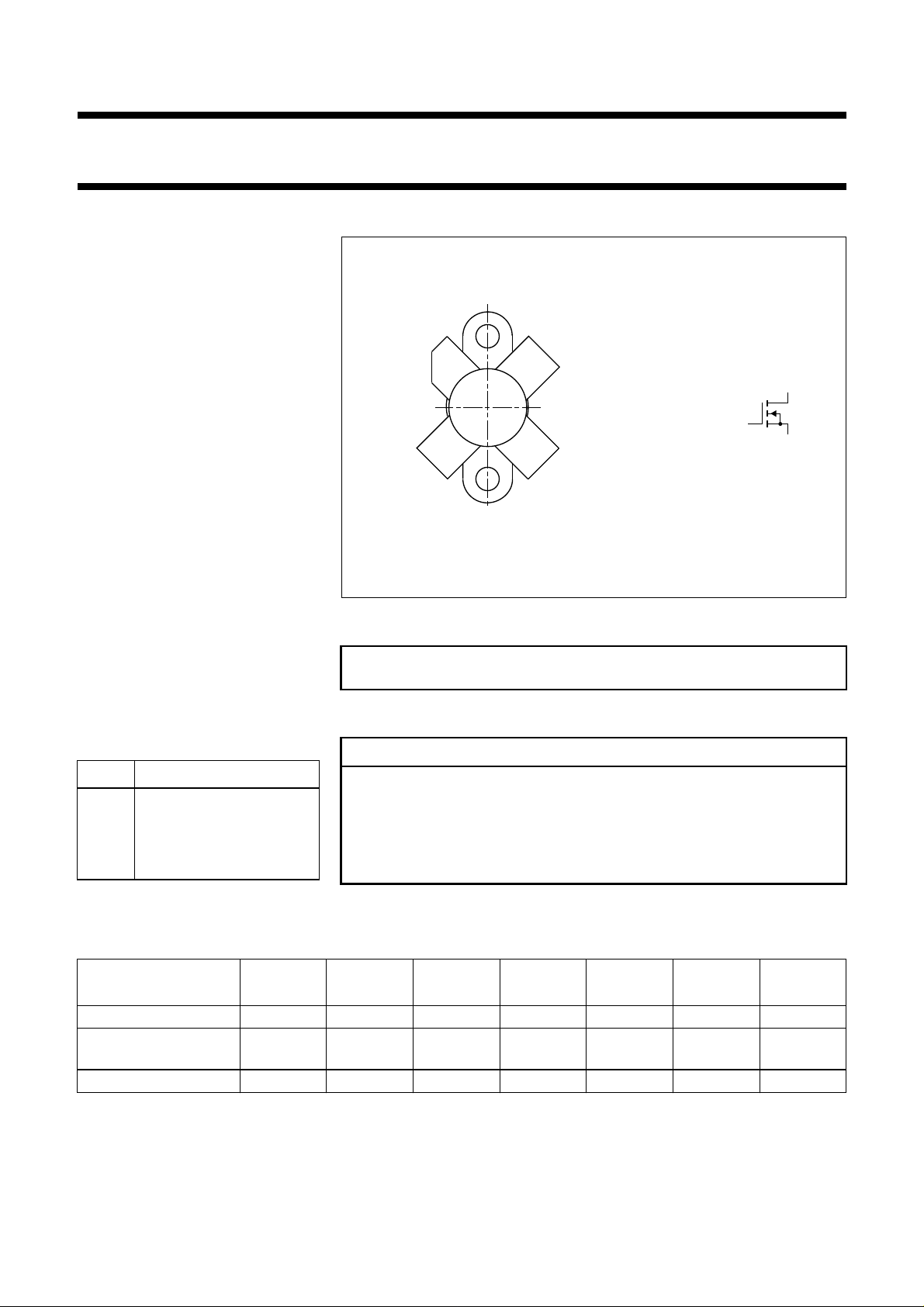
The transistor has a 4-lead, SOT123
flange envelope, with a ceramic cap.
All leads are isolated from the flange.
A marking code, showing gate-source
voltage (V
) information is provided
GS
for matched pair applications. Refer
to the 'General' section for further
information.
PIN CONFIGURATION
ok, halfpage
1
23
4
MSB057
g
MBB072
d
s
Fig.1 Simplified outline and symbol.
CAUTION
The device is supplied in an antistatic package. The gate-source input must
be protected against static charge during transport and handling.
WARNING
PINNING - SOT123
PIN DESCRIPTION
1 drain
2 source
3 gate
4 source
Product and environmental safety - toxic materials
This product contains beryllium oxide. The product is entirely safe provided
that the BeO disc is not damaged. All persons who handle, use or dispose of
this product should be aware of its nature and of the necessary safety
precautions. After use, dispose of as chemical or special waste according to
the regulations applying at the location of the user. It must never be thrown
out with the general or domestic waste.
QUICK REFERENCE DATA
RF performance at T
MODE OF
OPERATION
= 25 °C in a common source test circuit.
h
(MH
f
)
Z
V
(V)
DS
I
DQ
(mA)
P
(W)
L
G
P
(dB)
η
(%)
D
d
(dB)
class-A 28 50 800 8 (PEP) > 24 −<−40
class-AB 28 50 150 30 (PEP) typ. 24 typ. 40
typ. −35
(note 1)
CW, class-B 108 50 30 30 typ. 20 typ. 65 −
Note
1. 2-tone efficiency.
3
September 1992 2
Page 3
Philips Semiconductors Product specification
HF/VHF power MOS transistor BLF175
LIMITING VALUES
In accordance with the Absolute Maximum System (IEC 134).
SYMBOL PARAMETER CONDITIONS MIN. MAX. UNIT
V
DS
±V
GS
I
D
P
tot
T
stg
T
j
THERMAL RESISTANCE
drain-source voltage − 110 V
gate-source voltage − 20 V
DC drain current − 4A
total power dissipation up to Tmb = 25 °C − 68 W
storage temperature −65 150 °C
junction temperature − 200 °C
SYMBOL PARAMETER CONDITIONS
R
th j-mb
R
th mb-h
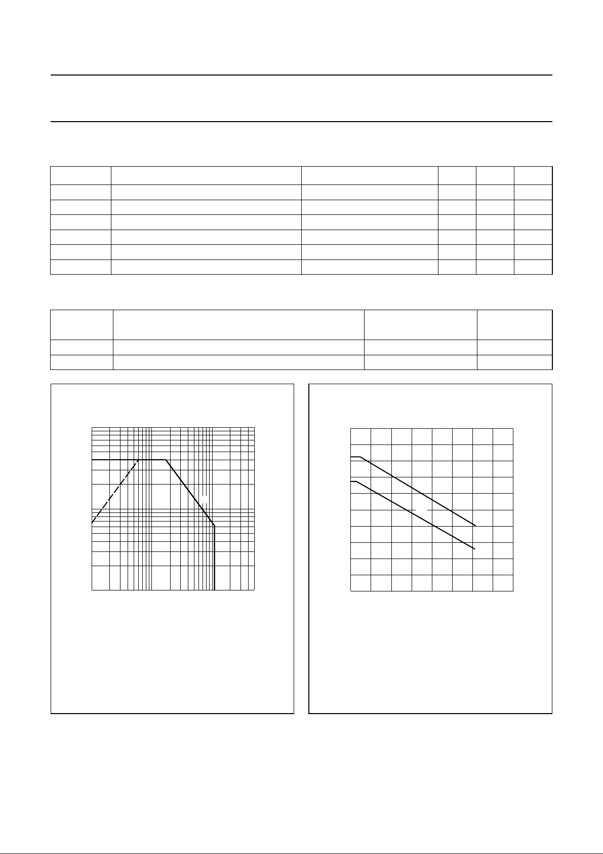
10
handbook, halfpage
I
D
(A)
1
−1
10
thermal resistance from junction to mounting base Tmb = 25 °C; P
thermal resistance from mounting base to heatsink Tmb = 25 °C; P
MRA905
(1)
110
(2)
VDS (V)
2
10
100
handbook, halfpage
P
tot
(W)
80
60
40
20
0
0 40 80 160
(2)
(1)
THERMAL
RESISTANCE
= 68 W 2.6 K/W
tot
= 68 W 0.3 K/W
tot
MGP063
120
T
(°C)
h
(1) Current is this area may be limited by R
(2) Tmb = 25 °C.
DS(on)
.
Fig.2 DC SOAR.
September 1992 3
(1) Continuous operation.
(2) Short-time operation during mismatch.
Fig.3 Power/temperature derating curves.
Page 4
Philips Semiconductors Product specification
HF/VHF power MOS transistor BLF175
CHARACTERISTICS
T
= 25 °C unless otherwise specified.
j
SYMBOL PARAMETER CONDITIONS MIN. TYP. MAX. UNIT
V
(BR)DSS
I
DSS
I
GSS
V
GS(th)
∆V
GS
g
fs
R
DS(on)
I
DSX
C
is
C
os
C
rs
drain-source breakdown voltage ID = 10 mA; VGS = 0 110 −− V
drain-source leakage current VGS = 0; VDS = 50 V −−100 µA
gate-source leakage current ±VGS = 20 V; VDS = 0 −−1µA
gate-source threshold voltage ID = 10 mA; VDS = 10 V 2 − 4.5 V
gate-source voltage difference of
ID = 10 mA; VDS = 10 V −−100 mV
matched pairs
forward transconductance ID = 1 A; VDS = 10 V 1.1 1.6 − S
drain-source on-state resistance ID = 1 A; VGS = 10 V − 0.75 1.5 Ω
on-state drain current VGS = 10 V; VDS = 10 V − 5.5 − A
input capacitance VGS = 0; VDS = 50 V; f = 1 MHz − 130 − pF
output capacitance VGS = 0; VDS = 50 V; f = 1 MHz − 36 − pF
feedback capacitance VGS = 0; VDS = 50 V; f = 1 MHz − 3.7 − pF
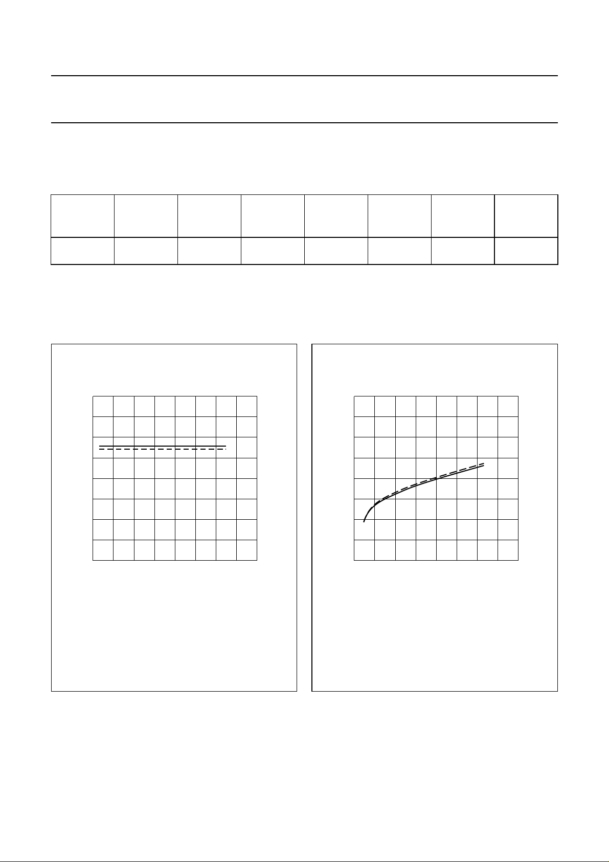
handbook, halfpage
0
T.C.
(mV/K)
−1
−2
−3
−4
−5
10
VDS= 10 V.
−2
−1
10
ID (A)
Fig.4 Temperature coefficient of gate-source
voltage as a function of drain current, typical
values.
MGP064
GS
MGP065
(V)
handbook, halfpage
1
6
I
D
(A)
4
2
0
0
VDS= 10 V; Tj=25°C.
510
V
Fig.5 Drain current as a function of gate-source
voltage, typical values.
September 1992 4
Page 5
Philips Semiconductors Product specification
HF/VHF power MOS transistor BLF175
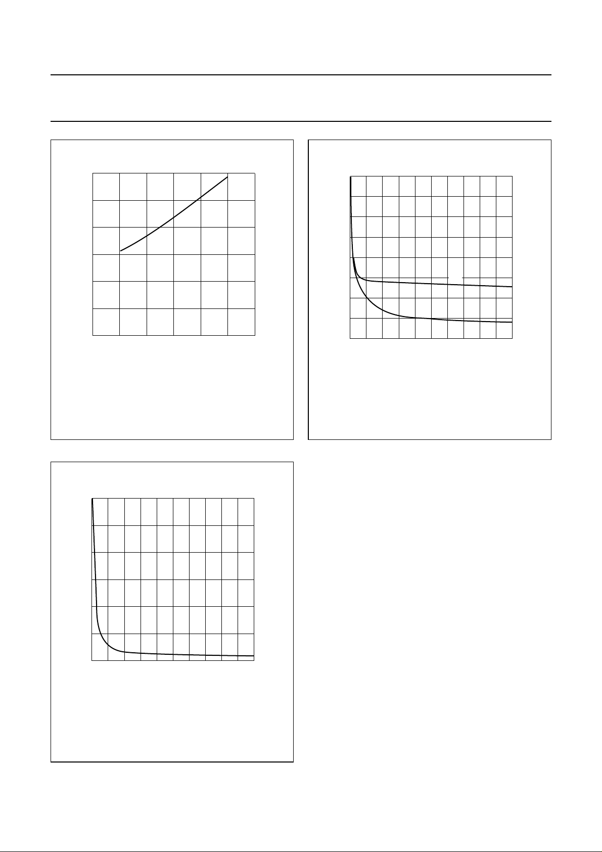
1.5
handbook, halfpage
R
DS(on)
(Ω)
1
0.5
0
0 50 100 150
ID= 1 A; VGS= 10 V.
Tj (°C)
Fig.6 Drain-source on-state resistance as a
function of junction temperature, typical
values.
MGP066
400
handbook, halfpage
C
(pF)
300
200
100
0
0
VGS= 0; f = 1 MHz.
C
is
C
os
10 50
20 30 40
MGP067
VDS (V)
Fig.7 Input and output capacitance as functions
of drain-source voltage, typical values.
150
handbook, halfpage
C
rs
(pF)
100
50
0
0
VGS= 0; f = 1 MHz.
10 50
20 30 40
V
Fig.8 Feedback capacitance as a function of
drain-source voltage, typical values.
MGP068
DS
(V)
September 1992 5
Page 6
Philips Semiconductors Product specification
HF/VHF power MOS transistor BLF175
APPLICATION INFORMATION FOR CLASS-A OPERATION
T
= 25 °C; R
h
RF performance in SSB operation in a common source circuit.
f
= 28.000 MHz; f2 = 28.001 MHz.
1
= 0.3 K/W; unless otherwise specified.
th mb-h
P
(W)
L
f
(MHz)
V
(V)
DS
I
DQ
(mA)
G
(dB)
0 to 8 (PEP) 28 50 800 > 24
typ. 28
d
P
3
(dB)
(note 1)
>−40
typ. −44
d
5
(dB)
(note 1)
<−40
typ. −64
R
(Ω)
24
24
GS
Note
1. Stated figures are maximum values encountered at any driving level between the specified value of PEP and are
referred to the according level of either the equal amplified tones. Related to the according peak envelope power
these figures should be decreased by 6 dB.
40
handbook, halfpage
G
p
(dB)
30
20
MGP069
d
(dB)
−20
−40
0
3
handbook, halfpage
MGP070
10
0
0 5 10 20
Class-A operation; VDS = 50 V; IDQ = 0.8 A;
RGS = 24 Ω;f1 = 28.000 MHz; f2 = 28.001 MHz.
solid line: Th = 25 °C.
dotted line: Th = 70 °C.
15
PL (W) PEP
Fig.9 Power gain as a function of load power,
typical values.
September 1992 6
−60
−80
0 5 10 20
Class-A operation; VDS = 50 V; IDQ = 0.8 A;
RGS = 24 Ω;f1 = 28.000 MHz; f2 = 28.001 MHz.
solid line: Th = 25 °C.
dotted line: Th = 70 °C.
15
PL (W) PEP
Fig.10 Third order intermodulation distortion as a
function of load power, typical values.
Page 7

Philips Semiconductors Product specification
HF/VHF power MOS transistor BLF175
40
handbook, halfpage
G
p
(dB)
30
20
10
0
01020 40
Class-A operation; VDS = 50 V; IDQ = 0.8 A;
PL = 8 W (PEP); RGS = 24 Ω; f1− f2= 1 MHz.
30
f (MHz)
Fig.11 Power gain as a function of frequency,
typical values.
MGP071
30
MGP072
f (MHz)
−20
handbook, halfpage
d
3
(dB)
−40
−60
01020 40
Class-A operation; VDS = 50 V; IDQ = 0.8 A;
PL = 8 W (PEP); RGS = 24 Ω; f1− f2= 1 MHz.
Fig.12 Third order intermodulation distortion as a
function of frequency, typical values.
+V
R2
R1
L1
C3
G
handbook, full pagewidth
f = 28 MHz.
50 Ω
input
C1
T1
C2
Fig.13 Test circuit for class-A operation.
September 1992 7
C4
D.U.T.
C5
L4
C9
L2
C6
C7
R3
L3
C8
+V
MGP073
D
50 Ω
output
Page 8

Philips Semiconductors Product specification
HF/VHF power MOS transistor BLF175
List of components (class-A test circuit)
COMPONENT DESCRIPTION VALUE DIMENSIONS CATALOGUE NO.
C1 multilayer ceramic chip capacitor
(note 1)
C2 multilayer ceramic chip capacitor 3 × 10 nF 2222 852 47103
C3, C4, C6 multilayer ceramic chip capacitor 100 nF 2222 852 47104
C5 multilayer ceramic chip capacitor 10 nF 2222 852 47103
C7 multilayer ceramic chip capacitor 3 × 100 nF 2222 852 47104
C8 aluminium electrolytic capacitor 10 µF, 63 V 2222 030 28109
C9 multilayer ceramic chip capacitor
(note 1)
L1 4 turns enamelled 0.6 mm copper
wire
L2 36 turns enamelled 0.7 mm copper
wire wound on a rod grade 4B1
Ferroxcube drain choke
L3 grade 3B Ferroxcube wideband RF
choke
L4 8 turns enamelled 1 mm copper wire 189 nH length 9.5 mm;
R1 0.4 W metal film resistor 24 Ω
R2 0.4 W metal film resistor 1500 Ω
R3 0.4 W metal film resistor 10 Ω
T1 4 : 1 transformer; 18 turns twisted
pair of 0.25 mm copper wire with
10 twists per cm, wound on a grade
4C6 toroidal core
39 pF
24 pF
86 nH length 3.3 mm;
int. dia. 5 mm;
leads 2 x 2 mm
20 µH length 30 mm;
int. dia. 5 mm
int. dia. 5 mm;
leads 2 x 3 mm
dimensions
9 x 6 x 3 mm
4330 030 30031
4312 020 36640
4322 020 97171
Note
1. American Technical Ceramics (ATC) capacitor, type 100B or other capacitor of the same quality.
September 1992 8
Page 9

Philips Semiconductors Product specification
HF/VHF power MOS transistor BLF175
handbook, full pagewidth
mounting screw
strap
100
90
strap
L3
+V
R3
DD
C8
L4
C9
MGP074
+V
G
L1
C3
R1
T1
C2
C1
R2
Note: The circuit and components are situated on one side of the epoxy fibre-glass board, the other side being
fully metallized to serve as earth. Earth connections are made by means of hollow rivets and straps at the two
edges and under the source contacts.
C6
L2
C7
C5
C4
Fig.14 Component layout for 28 MHz class-A test circuit.
September 1992 9
Page 10

Philips Semiconductors Product specification
HF/VHF power MOS transistor BLF175
APPLICATION INFORMATION FOR CLASS-AB OPERATION
T
= 25 °C; R
h
RF performance in SSB operation in a common source circuit.
f
= 28.000 MHz; f2 = 28.001 MHz.
1
= 0.3 K/W; unless otherwise specified.
th mb-h
P
(W)
L
f
(MHz)
V
(V)
DS
I
DQ
(mA)
G
P
(dB)
30 (PEP) 28 50 150 typ. 24 typ. 40
(note 2)
Notes
1. Stated figures are maximum values encountered at
any driving level between the specified value of PEP
and are referred to the according level of either the
equal amplified tones. Related to the according peak
envelope power these figures should be decreased by
6 dB.
2. 2-tone efficiency.
Ruggedness in class-AB operation
The BLF175 is capable of withstanding a load mismatch
corresponding to VSWR = 50 through all phases at
P
= 30 W single tone under the following conditions:
L
VDS = 50 V; f = 28 MHz.
28
handbook, halfpage
G
p
(dB)
26
MGP076
60
handbook, halfpage
η
D
(%)
50
η
(%)
d
D
3
(dB)
(note 1)
d
5
(dB)
(note 1)
R
(Ω)
GS
typ. −35 typ. −40 22
MGP077
24
22
20
0 204060
Class-AB operation; VDS = 50 V; IDQ = 0.15 A;
RGS = 22 Ω;f1 = 28.000 MHz; f2 = 28.001 MHz.
PL (W) PEP
Fig.15 Power gain as a function of load power,
typical values.
September 1992 10
40
30
20
0 204060
Class-AB operation; VDS = 50 V; IDQ = 0.15 A;
RGS = 22 Ω;f1 = 28.000 MHz; f2 = 28.001 MHz.
PL (W) PEP
Fig.16 Two tone efficiency as a function of load
power, typical values.
Page 11

Philips Semiconductors Product specification
HF/VHF power MOS transistor BLF175
handbook, halfpage
0
d
3
(dB)
−20
−40
−60
0 204060
Class-AB operation; VDS = 50 V; IDQ = 0.15 A;
RGS = 22 Ω;f1 = 28.000 MHz; f2 = 28.001 MHz.
MGP078
PL (W) PEP
Fig.17 Third order intermodulation distortion as a
function of load power, typical values.
handbook, halfpage
0
d
5
(dB)
−20
−40
−60
0 204060
Class-AB operation; VDS = 50 V; IDQ = 0.15 A;
RGS = 22 Ω;f1 = 28.000 MHz; f2 = 28.001 MHz.
MGP079
PL (W) PEP
Fig.18 Fifth order intermodulation distortion as a
function of load power, typical values.
handbook, full pagewidth
50 Ω
output
f = 28 MHz.
C1
C2
C3
C4
R2
L1
+V
L2
R1
C5
G
D.U.T.
Fig.19 Test circuit for class-AB operation.
September 1992 11
C6
C10
L3
C7
L5
L4
R3
L6
C8
C11
C9
C12
output
+V
D
MGP080
50 Ω
Page 12

Philips Semiconductors Product specification
HF/VHF power MOS transistor BLF175
List of components (class-AB test circuit)
COMPONENT DESCRIPTION VALUE DIMENSIONS CATALOGUE NO.
C1, C10 multilayer ceramic chip capacitor
(note 1)
C2, C4, C8, C11 film dielectric trimmer 5 to 60 pF 2222 809 07011
C3 multilayer ceramic chip capacitor
(note 1)
C5, C6, C9 multilayer ceramic chip capacitor 100 nF 2222 852 47104
C7 multilayer ceramic chip capacitor
(note 1)
C12 aluminium electrolytic capacitor 10 µF, 63 V 2222 030 28109
L1 9 turns enamelled 1 mm copper wire 280 nH length 11 mm;
L2, L3 stripline (note 2) 30 Ω length 10 mm;
L4 14 turns enamelled 1 mm copper
wire
L5 10 turns enamelled 1 mm copper
wire
L6 grade 3B Ferroxcube wideband RF
choke
R1 0.4 W metal film resistor 22 Ω
R2 0.4 W metal film resistor 1 MΩ
R3 0.4 W metal film resistor 10 Ω
62 pF
51 pF
10 pF
int. dia. 6 mm;
leads 2 x 4 mm
width 6 mm
1650 nH length 20 mm;
int. dia. 12 mm;
leads 2 x 2 mm
380 nH length 13 mm;
int. dia. 7 mm;
leads 2 x 3 mm
4312 020 36640
Notes
1. American Technical Ceramics (ATC) capacitor, type 100B or other capacitor of the same quality.
2. The striplines are on a double copper-clad printed circuit board, with PTFE fibre-glass dielectric (ε
thickness 1.6 mm.
September 1992 12
= 4.5),
r
Page 13

Philips Semiconductors Product specification
HF/VHF power MOS transistor BLF175
handbook, full pagewidth
strap
mounting screw
C2 C4
150
strap
rivet
R3
C9
R2
C5
R1
L1
L2 L3
C3C1
C6
L6
L4
L5
C7
C12
C8 C11
strap
70
C10
Note: The circuit and components are situated on one side of the epoxy fibre-glass board, the other side being
fully metallized to serve as earth. Earth connections are made by means of hollow rivets and straps at the two
edges and under the source contacts.
Dimensions in mm.
Fig.20 Component layout for 28 MHz class-AB test circuit.
September 1992 13
MGP081
Page 14

Philips Semiconductors Product specification
HF/VHF power MOS transistor BLF175
30
MGP083
f (MHz)
30
handbook, halfpage
Z
i
(Ω)
20
10
0
−10
−20
01020 40
Class-AB operation; VDS= 50 V; IDQ= 0.15 A;
= 30 W (PEP); RGS=22Ω.
P
L
r
i
x
i
Fig.21 Input impedance as a function of frequency
(series components), typical values.
50
handbook, halfpage
Z
L
(Ω)
40
30
20
10
0
0102030
Class-AB operation; VDS= 50 V; IDQ= 0.15 A;
= 30 W (PEP); RGS=22Ω.
P
L
R
L
X
L
MGP084
f (MHz)
Fig.22 Load impedance as a function of frequency
(series components), typical values.
30
handbook, halfpage
G
p
(dB)
20
10
0
0 102030
Class-AB operation; VDS= 50 V; IDQ= 0.15 A;
= 30 W (PEP); RGS=22Ω.
P
L
f (MHz)
Fig.23 Power gain as a function of frequency,
typical values.
MGP085
September 1992 14
Page 15

Philips Semiconductors Product specification
HF/VHF power MOS transistor BLF175
APPLICATION INFORMATION FOR CLASS-AB OPERATION
RF performance in SSB operation in a common source circuit.
MODE OF
OPERATION
f
(MHz)
V
(V)
DS
I
DQ
(mA)
P
(W)
L
G
P
(dB)
η
(%)
D
R
(Ω)
CW, class-B 108 50 30 30 typ. 20 typ. 65 10
10
handbook, halfpage
Z
i
(Ω)
5
0
MGP086
r
i
x
i
50
handbook, halfpage
Z
L
(Ω)
40
30
20
10
X
L
R
L
MGP087
GS
−5
0
Class-B operation; VDS= 50 V; IDQ= 30 mA;
= 30 W; RGS=10Ω.
P
L
100
f (MHz)
200
Fig.24 Input impedance as a function of frequency
(series components), typical values.
0
0 200
Class-B operation; VDS= 50 V; IDQ= 30 mA;
= 30 W; RGS=10Ω.
P
L
100
f (MHz)
Fig.25 Load impedance as a function of frequency
(series components), typical values.
September 1992 15
Page 16

Philips Semiconductors Product specification
HF/VHF power MOS transistor BLF175
30
handbook, halfpage
G
p
(dB)
20
10
0
0
Class-B operation; VDS= 50 V; IDQ= 30 mA;
= 30 W; RGS=10Ω.
P
L
100
f (MHz)
Fig.26 Power gain as a function of frequency,
typical values.
MGP088
200
September 1992 16
Page 17

Philips Semiconductors Product specification
HF/VHF power MOS transistor BLF175
PACKAGE OUTLINE
Flanged ceramic package; 2 mounting holes; 4 leads SOT123A
D
A
F
H
α
1
H
q
U
1
L
C
B
w
M
C
2
b
43
p
2
0 5 10 mm
scale
A
U
2
w
M
AB
1
c
U
3
Q
DIMENSIONS (millimetre dimensions are derived from the original inch dimensions)
5.82
5.56
c
Db
9.73
0.18
9.47
0.10
0.397
0.383
0.007
0.004
IEC JEDEC EIAJ
0.373
0.371
D
9.63
9.42
F
1
2.72
20.71
2.31
19.93
0.815
0.107
0.091
0.221
0.785
0.203
REFERENCES
5.61
5.16
pH
3.33
3.04
0.131
0.120
Q
4.63
4.11
0.182
0.162
q
18.42
0.725
U
1
25.15
24.38
0.99
0.96
U2U
6.61
6.09
0.26
0.24
w
1
3
9.78
9.39
0.385
0.370
EUROPEAN
PROJECTION
UNIT
inches
A
7.47
mm
6.37
0.229
0.294
0.219
0.251
OUTLINE
VERSION
SOT123A 97-06-28
September 1992 17
w
2
1.020.51
0.040.02
ISSUE DATE
αL
45°
Page 18

Philips Semiconductors Product specification
HF/VHF power MOS transistor BLF175
DEFINITIONS
Data Sheet Status
Objective specification This data sheet contains target or goal specifications for product development.
Preliminary specification This data sheet contains preliminary data; supplementary data may be published later.
Product specification This data sheet contains final product specifications.
Limiting values
Limiting values given are in accordance with the Absolute Maximum Rating System (IEC 134). Stress above one or
more of the limiting values may cause permanent damage to the device. These are stress ratings only and operation
of the device at these or at any other conditions above those given in the Characteristics sections of the specification
is not implied. Exposure to limiting values for extended periods may affect device reliability.
Application information
Where application information is given, it is advisory and does not form part of the specification.
LIFE SUPPORT APPLICATIONS
These products are not designed for use in life support appliances, devices, or systems where malfunction of these
products can reasonably be expected to result in personal injury. Philips customers using or selling these products for
use in such applications do so at their own risk and agree to fully indemnify Philips for any damages resulting from such
improper use or sale.
September 1992 18
 Loading...