

Datasheet BL3406B-1.0V, BL3406B-1.2V, BL3406B-1.5V, BL3406B-1.8V, BL3406B-2.5V Datasheet (Belling) [ru]
...Page 1

BL3406B
V
µ H
1.5 MHz, 800mA Synchronous Buck Converter
FEATURES
• High Efficiency: Up to 96%
• 1.5MHz Constant Switching Frequency
• Current Mode Operation for Excellent
Line and Load Transient Response
• No Schottky Diode Required
• 2.5V to 5.5V Input Voltage Range
• 1.0V,1.2V,1.5V,1.8V,2.5V and 3.3V
Fixed/Adjustable Output Voltage
• 100% Duty Cycle in Dropout Mode
• Low Quiescent Current: 180µA
• Over temperature Protection
• Short Circuit Protection
• Shutdown Quiescent Current < 1µA
• Space Saving 5-Pin Thin SOT23 Package
APPLICATIONS
• Cellular and Smart Phones
• Wireless Handsets and DSL Modems
• Microprocessors and DSP Core Supplies
• PDAs
• Digital Still and Video Cameras
• GPS Receivers
DESCRIPTION
The BL3406B is a constant frequency,
1.5MHz, slope compensated current mode
PWM step-down converter working under an
input voltage range of 2.5V to 5.5V. This
feature makes the BL3406B suitable for
single cell Li-ion battery-powered applications.
The internal synchronous rectifier is desired
to increase efficiency without an external
Schottky diode. 100% duty cycle capability
extends battery life in portable devices, while
the quiescent current is 180µA at no load,
and drops to < 1µA in shutdown. Pulse
Skipping Mode operation increases efficiency
at light loads, further extending battery life.
The BL3406B is offered in a low profile (1mm)
5-pin, thin SOT23 package, and is available
in an adjustable version and fixed output
versions of 1.0V, 1.2V, 1.5V , 1.8V, 2.5V and
3.3V.
• MP3/MP4/MP5 Players
• Portable Instruments
ORDERING INFORMATION TYPICAL APPLICATION
BL3406B –XX X XXX
Package:
TRN: TSOT23-5
RN: SOT23-5
Features:
P: Standard (default,
lead free)
C: Customized
Output Voltage:
10: 1.0V
12: 1.2V
15: 1.5V
18: 1.8V
25: 2.5V
33: 3.3V
AD: Adjustable
V
IN
2.7V - 4.2V
C1
4.7uF
4
IN
BL3406B-ADJ
1
Run
GND
SW
V
FB
2
L1
2.2
3
C3
22pF
5
R2
200k
R1
100k
Figure 1. BL3406B-ADJ Typical Application Circuit
V
1.8V
OUT
C2
10uF
PPMIC BU www.belling.com.cn
BL3406B Rev 1.5 Belling Proprietary Information. Unauthorized Photocopy and Duplication Prohibited
10/2009 ©2009 Belling All Rights Reserved
1
Page 2

BL3406B
1.5 MHz, 800mA Synchronous Buck Converter
Absolute Maximum Rating
Input Supply Voltage…………………-0.3V to +6V
RUN, VFB Voltages……………………-0.3V to +VIN
SW Voltages……………………-0.3V to (VIN+0.3V)
P-Channel Switch Source Current (DC) ………1A
N-Channel Switch Sink Current (DC) …………1A
(Note 1)
Peak SW Sink and Source Current……………1.4A
Operating Temperature Range……-40°C to +85°C
Junction Temperature
(Note2)
………………+125°C
Storage Temperature Range………-65°C to +150°C
Lead Temperature (Soldering, 10s) ………+300°C
Package Information
Adjustable Output Version Fixed Output Versions
SOT23-5
TOP VIEW
V
RUN
GND
SW
1
2
3
MARKING
FB
5
4
V
IN
SOT23-5
TOP VIEW
RUN
GND
SW
1
2
3
MARKING
5
4
Part Number Top Mark Temp Range
BL3406B-Adj
A J Y W
(Note3)
-40°C to +85°C
Part Number Top Mark Temp Range
BL3406B-1.0V A A Y W
BL3406B-1.2V A B Y W
BL3406B-1.5V A C Y W
BL3406B-1.8V A D Y W
-40°C to +85°C
BL3406B-2.5V A E Y W
BL3406B-3.3V A F Y W
Y 9 A B C D
Year 2009 2010 2011 2012 2013
W 1 … 26 27 28 … 53 54
Week A … Y Z a … y z
Thermal Resistance
Package JA JC
TSOT23-5
SOT23-5
Note 1: Absolute Maximum Ratings are those values beyond which the life of a device may be impaired.
Note 2: TJ is calculated from the ambient temperature T
T
Note 3: Y: Year of wafer manufacturing W: Week of wafer manufacturing
Note 4: Thermal Resistance is specified with approximately 1 square of 1 oz copper.
= TA + (PD) x (220°C/W).
J
220°C/W
250°C/W
(Note 4)
110°C/W
130°C/W
and power dissipation P
A
according to the following formula:
D
V
OUT
V
IN
PPMIC BU www.belling.com.cn
BL3406B Rev 1.5 Belling Proprietary Information. Unauthorized Photocopy and Duplication Prohibited
10/2009 ©2009 Belling All Rights Reserved
2
Page 3
1.5 MHz, 800mA Synchronous Buck Converter
Pin Description
PIN NAME FUNCTION
Regulator Enable Control Input. Drive RUN above 1.5V to turn on the part.
1 RUN
2 GND Ground
3 SW
4 VIN
5 VFB/V
Drive RUN below 0.3V to turn it off. In shutdown, all functions are disabled
drawing <1µA supply current. Do not leave RUN floating.
Power Switch Output. It is the switch node connection to external inductor. This
pin connects to the drains of the internal P-Channel and N-Channel MOSFET
switches.
Supply Input Pin. Must be closely decoupled to GND, Pin 2, with a 2.2µF or
greater ceramic capacitor.
VFB (BL3406B-Adj): Feedback Input Pin. Connect FB to the center point of the
external resistor divider. The regulated voltage on this pin is 0.6V.
V
OUT
(BL3406B-1.2/BL3406B-1.5/BL3406B-1.8): Output Voltage Feedback Pin.
OUT
An internal resistive divider divides the output voltage down for comparison to the
internal reference voltage.
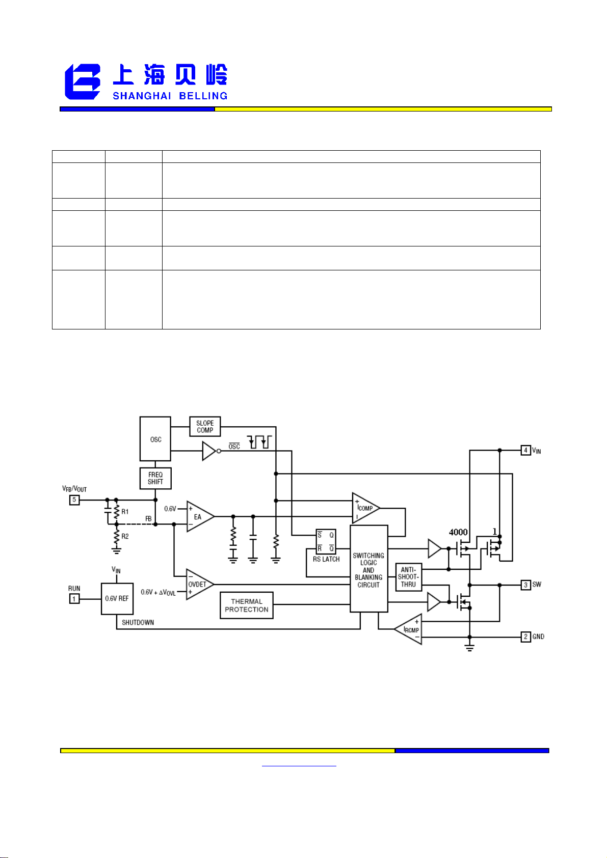
Block Diagram
BL3406B
PPMIC BU www.belling.com.cn
BL3406B Rev 1.5 Belling Proprietary Information. Unauthorized Photocopy and Duplication Prohibited
10/2009 ©2009 Belling All Rights Reserved
3
Page 4
BL3406B
1.5 MHz, 800mA Synchronous Buck Converter
Electrical Characteristics
(VIN =V
Input Voltage Range 2.5 5.5 V
Input DC Supply Current
Regulated Feedback
VFB Input Bias Current VFB = 0.65V ±30 nA
= 3.6V, TA = 25°C, unless otherwise noted.)
RUN
Parameter Conditions MIN TYP MAX Unit
Active Mode
Shutdown Mode
Voltage
VFB=0.5V or V
VFB=0V, VIN=4.2V
TA= -40°C ≤ TA ≤ 85°C 0.5850 0.6000 0.6150
(Note 5)
=90%
OUT
TA = +25°C 0.5880 0.6000 0.6120
TA= 0°C ≤ TA ≤ 85°C 0.5865 0.6000 0.6135
180
0.1
300
1.0
µA
µA
V
V
V
Reference Voltage Line
Regulation
Regulated Output Voltage
Output Overvoltage
Lockout
Output Voltage Line
Regulation
Output Voltage Load
Regulation
Peak Inductor Current
Oscillator Frequency VFB=0.6V or V
R
R
Note 5: 100% production test at +25°C. Specifications over the temperature range are guaranteed by design and
characterization.
of P-CH MOSFET
DS(ON)
of N-CH MOSFET
DS(ON)
SW Leakage Current V
RUN Threshold -40°C ≤ TA ≤ 85°C 0.3 1.1 1.30 V
RUN Leakage Current ±0.01
BL3406B-1.2, -40°C ≤ TA ≤ 85°C 1.164 1.200 1.236
BL3406B-1.8, -40°C ≤ TA ≤ 85°C 1.746 1.800 1.854
∆V
OVL
∆V
RUN
VIN = 2.5V to 5.5V 0.04 0.4 %/V
= V
OVL
VIN=3V, VFB=0.5V or V
– VFB, Adjustable Version
OVL
= V
= 0V, VSW= 0V or 5V, VIN = 5V ±0.01
– V
OVL
VIN = 2.5V to 5.5V 0.04 0.40 %
Duty Cycle <35%
I
SW
ISW = -300mA 0.35 0.45 Ω
, Fixed Version 2.5 7.8 13 %
OUT
0.5 %
=90%
OUT
=100% 1.2 1.5 1.8 MHz
OUT
= 300mA 0.40 0.50 Ω
20 50 80 mV
1.2 A
V
V
±1 µA
±1 µA
PPMIC BU www.belling.com.cn
BL3406B Rev 1.5 Belling Proprietary Information. Unauthorized Photocopy and Duplication Prohibited
10/2009 ©2009 Belling All Rights Reserved
4
Page 5

1.5 MHz, 800mA Synchronous Buck Converter
Typical Performance Characteristics
(Test Figure 1 above unless otherwise specified)
BL3406B
Efficiency vs. Output Current
90
V
OUT
=1.8V
L=2.2uH
80
70
60
50
Efficiency(%)
40
30
20
0.1 1 10 100 1000
Vin=2.7V
Vin=3.6V
Vin=4.2V
Output Current(mA)
0.606
Reference Voltage vs. Temperature
VIN=3.6V
0.605
0.604
Reference Voltage(V)
0.603
0.602
-50 -25 0 25 50 75 100 125
Temperature(°C
)
Supply Current vs. Supply Voltage Start_up from Shutdown
245
V
OUT
240
235
230
225
220
215
210
205
Dynamic Supply Current(uA)
200
195
=1.8V
I
LOAD
=0A
TA=25°C
2 3 4 5 6
Supply Voltage(V)
2.2
Output Voltage vs. Load Current
VIN=3.6V
2.1
TA=25°C
2.0
1.9
1.8
1.7
1.6
Output Voltage(V)
1.5
1.4
1.3
0 200 400 600 800 1000 1200
Load Current(mA)
Output Voltage vs. Input Voltage
1.820
I
LOAD
1.815
1.810
1.805
(V)
1.800
OUT
V
1.795
1.790
1.785
1.780
2.7 3.0 3.3 3.6 3.9 4.2 4.5 4.8 5.1 5.4 5.7
I
I
LOAD
LOAD
=10mA
=100mA
=600mA
VIN(V)
PPMIC BU www.belling.com.cn
BL3406B Rev 1.5 Belling Proprietary Information. Unauthorized Photocopy and Duplication Prohibited
5
10/2009 ©2009 Belling All Rights Reserved
Page 6

Load Step
1.5 MHz, 800mA Synchronous Buck Converter
BL3406B
Load Step
Pulse Skipping Mode
Load Step
Load Step
Output Short
PPMIC BU www.belling.com.cn
BL3406B Rev 1.5 Belling Proprietary Information. Unauthorized Photocopy and Duplication Prohibited
10/2009 ©2009 Belling All Rights Reserved
6
Page 7

1.5 MHz, 800mA Synchronous Buck Converter
Operation
The BL3406B uses a constant frequency,
current mode step-down architecture. Both
the main switch (P-channel MOSFET) and
the synchronous rectifier (N-channel
MOSFET) are integrated internally. This
Step-Down DC-DC Converter can supply
800mA output current over a wide input
voltage range from 2.5V to 5.5V. The over
voltage comparator OVDET guards against
transient overshoots >7.8% by turning the
main switch off and keeping it off until the
fault is removed.
Current Mode PWM Control
Slope compensated current mode PWM
control provides stable switching and cycleby-cycle current limit for excellent load and
line responses. During normal operation, the
internal main switch is turned on for a certain
time to ramp the inductor current at each
rising edge of the internal oscillator, and
turned off when the peak inductor current
reaches the controlled value. When the main
switch is off, the synchronous rectifier will be
turned on immediately and stay on until either
the inductor current starts to reverse, as
indicated by the current reversal comparator,
I
, or the beginning of the next clock cycle.
RCMP
Pulse Skipping Mode Operation
At very light loads, the BL3406B will
automatically enter Pulse Skipping Mode to
increase efficiency, further extending battery
life. In this mode, the control loop skips PWM
pulses while maintaining output in regulation,
and the switching frequency depends on the
load condition. This is a kind of PFM mode
operation.
Dropout Operation
When the input voltage decreases toward the
BL3406B
value of the output voltage, the BL3406B will
keep the main switch on for more than one
switching cycle and increases the duty cycle
(Note 6) until it reaches 100%. The output
voltage then is the input voltage minus the
voltage drop across the main switch and the
inductor. At low input supply voltage, the
R
and the efficiency of the converter decreases.
Caution must be exercised to ensure the heat
dissipated not to exceed the maximum
junction temperature of the IC.
Note 6666: The duty cycle D of a step-down converter is
defined as:
where TON is the main switch on time, and f
is the oscillator frequency (1.5MHz).
Short Circuit Protection
The BL3406B has short circuit protection.
When output is shorted to ground, the
oscillator frequency is reduced to prevent the
inductor current from increasing beyond the
PFET current limit. The PFET current limit is
also reduced to lower the short circuit current.
The frequency and current limit will return to
the normal values once the short circuit
condition is removed and the feedback
voltage reaches 0.6V.
Maximum Load Current
The BL3406B will operate with input supply
voltage as low as 2.5V, however the
maximum load current decreases at lower
input voltage due to large IR drop on the
main switch and synchronous rectifier.
of the P-Channel MOSFET increases,
DS(ON)
V
fTD
OSCON
V
OUT
IN
%100%100 ×≈××=
OSC
PPMIC BU www.belling.com.cn
BL3406B Rev 1.5 Belling Proprietary Information. Unauthorized Photocopy and Duplication Prohibited
10/2009 ©2009 Belling All Rights Reserved
7
Page 8

V
µ H
1
R
Application Information
Figure 2 below shows the basic application
circuit with BL3406B fixed output versions.
V
IN
2.7V - 4.2V
C1
4.7uF
4
IN
BL3406B-18
1
Run
SW
V
GND
2
Figure 2. Basic Application Circuit
with fixed output versions
Setting the Output Voltage
Figure 1 above shows the basic application
circuit with BL3406B adjustable output
version. The external resistor sets the output
voltage according to the following equation:
2
R
OUT
1(6.0
VV
)
+×=
Table 1—Resistor Selection vs.
Output Voltage Setting
VOUT R1 R2
1.0V 180 k
1.2V 180 k
1.5V 180 k
1.8V 180 k
2.5V 158 k
3.3V 180 k
Ω(1%)
Ω(1%)
Ω(1%)
Ω(1%)
Ω(1%)
Ω(1%)
Inductor Selection
The output inductor is selected to limit the
ripple current to some predetermined value,
typically 20%~40% of the full load current at
the maximum input voltage. In continuous
mode, the ripple current is determined by:
1
I −
=∆
A reasonable starting point for setting ripple
current is ∆IL=320mA (40% of 800mA). For
V
OUTL
Lf
×
L1
2.2
3
5
OUT
180 k
270 k
360 k
499 k
810 k
V
OUT
V
IN
120 k
)1(
Ω(1%)
Ω(1%)
Ω(1%)
Ω(1%)
Ω(1%)
Ω(1%)
V
OUT
C2
10uF
BL3406B
1.5 MHz, 800mA Synchronous Buck Converter
output voltages above 2.0V, when efficiency
at light load condition is important, the
minimum recommended inductor is 2.2µH.
For optimum voltage-positioning load
transients, choose an inductor with DC series
resistance below 150mΩ. For higher
1.8V
efficiency at heavy loads (above 200mA), or
minimal load regulation (but some transient
overshoot), the resistance should be kept
below 100mΩ. The DC current rating of the
inductor should be at least equal to the
maximum load current plus half the ripple
current to prevent core saturation. Thus, a
1120mA rated inductor should be enough for
most applications (800mA+320mA).
Input Capacitor Selection
The input capacitor reduces the surge current
drawn from the input and switching noise
from the device. The input capacitor
impedance at the switching frequency shall
be less than input source impedance to
prevent high frequency switching current
passing to the input. In continuous mode, the
source current of the main switch is a square
wave of duty cycle V
OUT/VIN
. To prevent large
voltage transients, a low ESR input capacitor
sized for the maximum RMS current must be
used. The maximum RMS capacitor current is
given by:
VVV
−
II
≈
OMAXRMS
OUTINOUT
V
IN
This formula has a maximum at VIN =2V
where I
RMS
= I
/2. This simple worst-case
OUT
5.0
)]([
OUT
condition is commonly used for design
because even significant deviations do not
offer much relief. Ceramic capacitors with
X5R or X7R dielectrics are recommended
due to their low ESR and high ripple current.
Output Capacitor Selection
The output capacitor is required to keep the
output voltage ripple small and to ensure
regulation loop stability. The output capacitor
must have low impedance at the switching
,
PPMIC BU www.belling.com.cn
BL3406B Rev 1.5 Belling Proprietary Information. Unauthorized Photocopy and Duplication Prohibited
10/2009 ©2009 Belling All Rights Reserved
8
Page 9

V
V
V IN
µ H
V
frequency. Ceramic capacitors with X5R or
X7R dielectrics are recommended due to
their low ESR and high ripple current. The
output ripple ∆V
≤∆
V
OUT
OUT
is determined by:
−×
VVV
××
OUTINOUT
ESR
LfV
1)(
+×
8
OSCOSCIN
××
Cf
2
Layout Considerations
When laying out the printed circuit board, the
following checklist should be used to ensure
proper operation of the BL3406B. These
items are also illustrated graphically in
Figures 5 and 6. Check the following in your
layout:
BL3406B
1.5 MHz, 800mA Synchronous Buck Converter
1. The power traces, consisting of the GND
trace, the SW trace and the VIN trace
should be kept short, direct and wide.
2. Does the VFB pin connect directly to the
feedback resistors? The resistive divider
R1/R2 must be connected between the (+)
plate of Cout and ground.
3. Does the (+) plate of CIN connect to VIN as
closely as possible? This capacitor
provides the AC current to the internal
power MOSFETS.
4. Keep the switching node, SW, away from
the sensitive V
5. Keep the (-) plates of CIN and C
close as possible.
node.
FB
OUT
as
2.7V - 4.2V
V
IN
C1
4.7uF
4
IN
BL3406B-ADJ
1
Run
GND
SW
V
FB
2
L1
2.2 µ H
3
C3
22pF
5
R2
200k
R1
100k
OUT
C2
10uF
1.8V
V
IN
2.7V - 4.2V
C1
4.7uF
4
BL3406B-18
1
Run
GND
SW
V
OUT
2
L1
2.2
3
5
Figure 3. BL3406B-ADJ Layout Circuit Figure 4. BL3406B-1.8 Layout Circuit
1.8V
OUT
C2
10uF
Figure 5. BL3406B-ADJ Suggested Layout Figure 6. BL3406B-1.8 Suggested Layout
PPMIC BU www.belling.com.cn
BL3406B Rev 1.5 Belling Proprietary Information. Unauthorized Photocopy and Duplication Prohibited
10/2009 ©2009 Belling All Rights Reserved
9
Page 10

Package Description
BL3406B
1.5 MHz, 800mA Synchronous Buck Converter
Symbol
A 0.889 1.295 0.035 0.051
A1 0.000 0.152 0.000 0.006
B 1.397 1.803 0.055 0.071
b 0.356 0.559 0.014 0.022
C 2.591 2.997 0.102 0.118
D 2.692 3.099 0.106 0.122
e 0.838 1.041 0.033 0.041
H 0.080 0.254 0.003 0.010
L 0.300 0.610 0.012 0.024
Dimensions In Millimeters Dimensions In Inches
Min Max Min Max
SOT-23-5 Surface Mount Package
PPMIC BU www.belling.com.cn
BL3406B Rev 1.5 Belling Proprietary Information. Unauthorized Photocopy and Duplication Prohibited
10/2009 ©2009 Belling All Rights Reserved
10
Page 11

BL3406B
1.5 MHz, 800mA Synchronous Buck Converter
TSOT-23-5 Surface Mount Package
PPMIC BU www.belling.com.cn
BL3406B Rev 1.5 Belling Proprietary Information. Unauthorized Photocopy and Duplication Prohibited
10/2009 ©2009 Belling All Rights Reserved
11
Page 12

 Loading...