Page 1

1
Mulimedia ICs
SCSI active terminator
BH9595FP-Y / BH9596FP-Y
These SCSI active terminators, developed as a substitute for conventional discrete terminators, maintain good consistency between VM level (2.85V) and GND level (0V) and between VM level and VDD level, and have extremely
low power consumption, dropping to a maximum of 90 milliwatts at standby (compared to the maximum of 990 milliwatts used by conventional resistance terminators). These SCSI active terminators electrically control SCSI lines,
connecting and disengaging the terminating resistor by electrically controlling the enable pin. (The enable pin is
enabled at the HIGH level and switched to the High-Z state by the LOW level in the BH9595 and by the HIGH level in
the BH9596, completely disconnecting the SCSI line from the SCSI terminator.)
These SCSI active terminators allow for the configuration of flexible, energy-saving SCSI networks, and are ideal for
notebook computers, hard disk drives and a wide range of other products with SCSI capabilities.
•
Applications
Compact disk drives, optical disk drives, CD-ROM drives, tape drives, personal computers (including laptop
computers and notebook computers), workstations,
mainframes, laser printers, plotters
•
Features
1) Internal 2.85V power supply and push-pull opera-
tion, for good consistency at all signal levels.
2) Enable pin for terminator enabling and disconnect-
ing, facilitating SCSI network construction.
3) Low power consumption, ideal for energy-saving
systems.
Power consumption during standby : 90mW (compared to 990mW for conventional resistor terminators)Power consumption at 25% duty : 614mW
(compared to 1,360mW for convention resistor terminators)Significant reductions in power consumption are possible.
4) Wide operating range.
TERM power : 4.0 ~ 5.5V (Transient : 6.0V)
5) Thin, microminiature design, ideal for space-saving
applications.
Package body size : 13.6 × 5.4 × 1.9mm
6) Active termination of 18-line SCSI.
7) Internal thermal shutdown circuit.
8) Compatibility with SCSI-I and SCSI-II.
Page 2

2
Mulimedia ICs BH9595FP-Y / BH9596FP-Y
•
Absolute maximum ratings (Ta = 25°C)
Power supply voltage
DC Output current
∗
1
DC Output current
∗
2
Input voltage
Power dissipation
∗
3
Operating temperature
Storage temperature
∗
2 Sink Current (from SCSI Line to Module) / Line
∗
1 Drain Current (from Module to SCSI Line) / Line
∗
3 When mounted to a 90 × 50 × 1.6 mm glass epoxy board
Parameter Symbol Limits Unit
V
DD1 V
I
SLD – 30 mA
I
SLS 35 mA
Vi V
1.45 W
Topr °C
Tstg °C
Pd
– 0.6 ~ (V
DD1
+ 0.6)
– 0.3 ~ + 7.0
0 ~ + 75
– 55 ~ + 125
•
Recommended operating conditions (Ta = 25°C)
Power supply voltage
Input voltage
Input voltage
SCSI Line voltage
∗
Transient 6V
Parameter Symbol Min. Typ. Max. Unit
V
DD1 4.0 4.5 5.5
∗
V
V
IH VDD1 – 0.6 — VDD1 + 0.6 V
V
IL – 0.3 — 0.8 V
V
SLX – 0.3 — VDD1 + 0.3 V
•
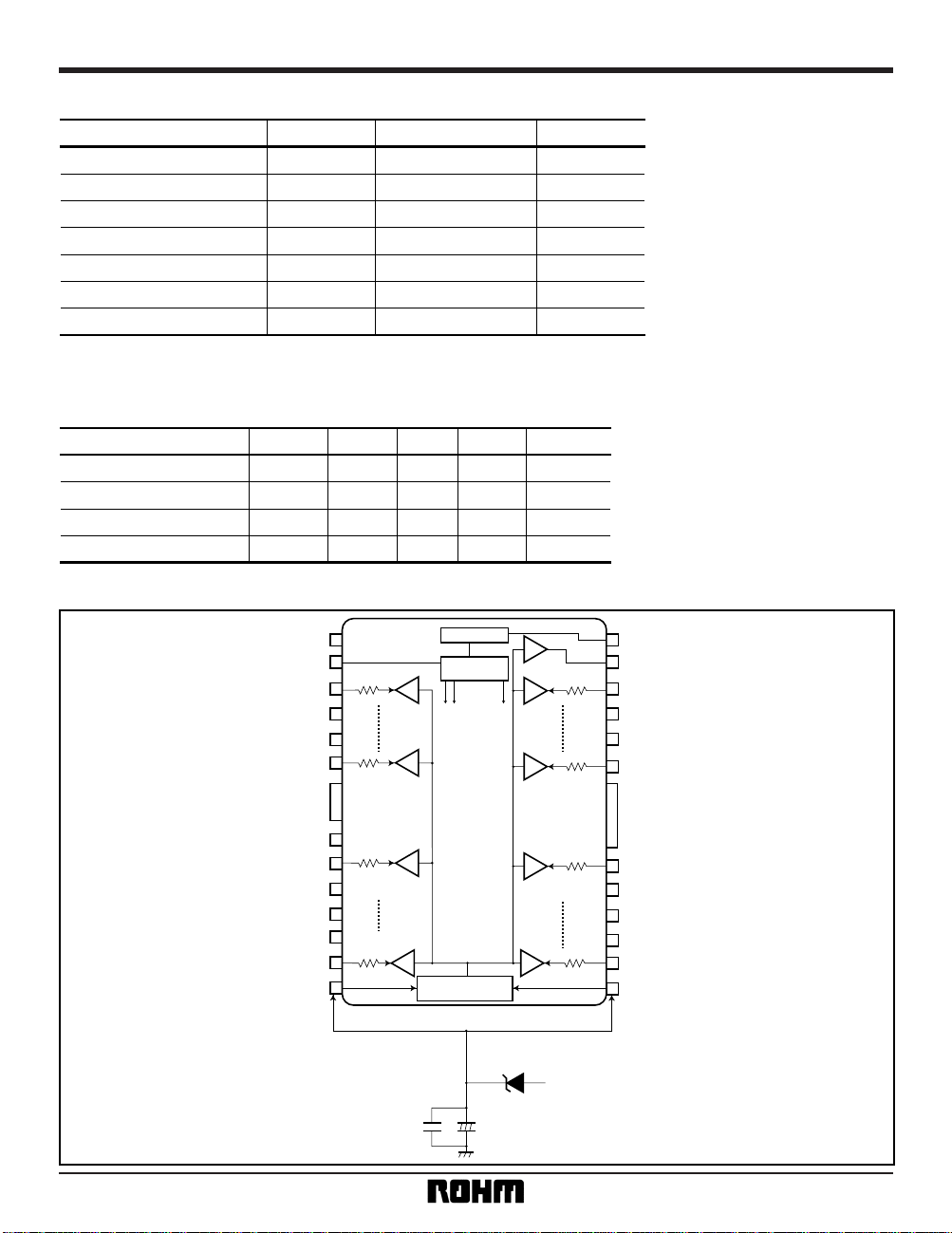
Block diagram
1
2
3
4
5
6
7
8
9
10
11
12
13
25
24
23
22
21
20
19
18
17
16
15
14
110Ω
Resistors
(PUSH - PULL)
(PUSH - PULL)
(PUSH - PULL)
POW
POW
POW
POW
POW
(PUSH - PULL)
(PUSH - PULL)
POW
POW
POW
(PUSH - PULL)
POW
to SW
2.85V SUPPLY
TSD
MODE
CONTROL
2.85V GENERATER
VDD1
SCSI LINE 6
SCSI LINE 7
SCSI LINE 8
SCSI LINE 9
SCSI LINE 10
GND
SCSI LINE 11
SCSI LINE 12
SCSI LINE 15
SCSI LINE 16
SCSI LINE 17
SCSI LINE 18
SCSI LINE 1
SCSI LINE 2
SCSI LINE 3
SCSI LINE 4
SCSI LINE 5
V
DD1
GND
GND
SCSI LINE 13
SCSI LINE 14
VM
TSD
Not to be used
(N.C.)
“H”: ENABLE
“L”: DISCONNECT
EN
(TRMPWR)
Schottky barrier diodes
SYSTEM POWER
5.0V
2.2
µ
0.1µ
+
–
∗
“L”: ENABLE
“H”: DISCONNECT
∗
For BH9596
BH9595FP-Y
Page 3

3
Mulimedia ICs BH9595FP-Y / BH9596FP-Y
•
Pin descriptions
Pin namePin name
14 VDD1
15
16
17
18
19
— GND
20
22
23
24 VM
25
21
1 (N.C.) Not to be used
2
3
4
5
6
— GND
7GND
8
9
10
11
12
13 V
DD1
Pin No. Pin No.
SCSI Line 15
SCSI Line 16
SCSI Line 17
SCSI Line 18
SCSI Line 1
SCSI Line 2
SCSI Line 3
SCSI Line 4
SCSI Line 5
SCSI Line 6
SCSI Line 7
SCSI Line 8
SCSI Line 9
SCSI Line 10
SCSI Line 11
SCSI Line 12
SCSI Line 13
SCSI Line 14
TSD (TSD signal output)
EN (Output enable)
•
Electrical characteristics
DC characteristics (unless otherwise noted, Ta = 25°C)
Input leakage current
SCSI equivalent resistance
SCSI line leakage current
SCSI line short current
∗
1
SCSI line short current
∗
2
VM voltage
Standby current
∗
1
SCSI total sink current
SCSI total drain current
Pin capacity
∗
3
∗
1 Drain Current (from Module to SCSI Line) / Line
∗
2 Sink Current (from SCSI Line to Module) / Line
∗
3 Guaranteed performance
∗
4 BH9595FP-Y: EN = GND, BH9595FP-Y: EN = VDD1
∗
5 BH9696FP-Y: EN = VDD1, BH9696FP-Y: EN = GND
Parameter Symbol Min. Typ. Max. Unit Conditions
I
IL 50 110 200 µA
I
IH – 1 — 1 µA
I
SLZ – 1 — 1 µA
I
SLD 15 25 30 mA
I
SLS 72030mA
V
M 2.700 2.85 3.000 V 4.0 ⬉ VDD1 ⬉ 5.5V
I
DDSTB — 1.0 2.0 mA
I
SLS 300 — 550 mA
I
SLD 300 — 550 mA
R
SL 105 — 115
Ω
PC — 5.0 6.0 pF
Vi = GND, V
DD1 = 5.5V
Vi = V
DD1, VDD1 = 5.5V
EN = ENABLE
∗
4
, VDD1 = 5.5V
EN = ENABLE
∗
4
, 4.0V ⬉ VDD1 ⬉ 5.5V
EN = ENABLE
∗
4
4.0 ⬉ VDD1 ⬉ 5.5V
4.0 ⬉ V
DD1 ⬉ 5.5V
4.0 ⬉ V
DD1 ⬉ 5.5V
4.0 ⬉ V
DD1 ⬉ 5.5V
EN = DISABLE
∗
5
, 18 SCSI Line = GND
EN = DISABLE
∗
5
, SCSI Line = GND,
EN = DISABLE
∗
5
, 18 SCSI Line = VDD1
EN = DISABLE
∗
5
, SCSI Line: VDD1 = 4.7V
EN = DISABLE
∗
5
, SCSI Line = VDD1
Page 4

4
Mulimedia ICs BH9595FP-Y / BH9596FP-Y
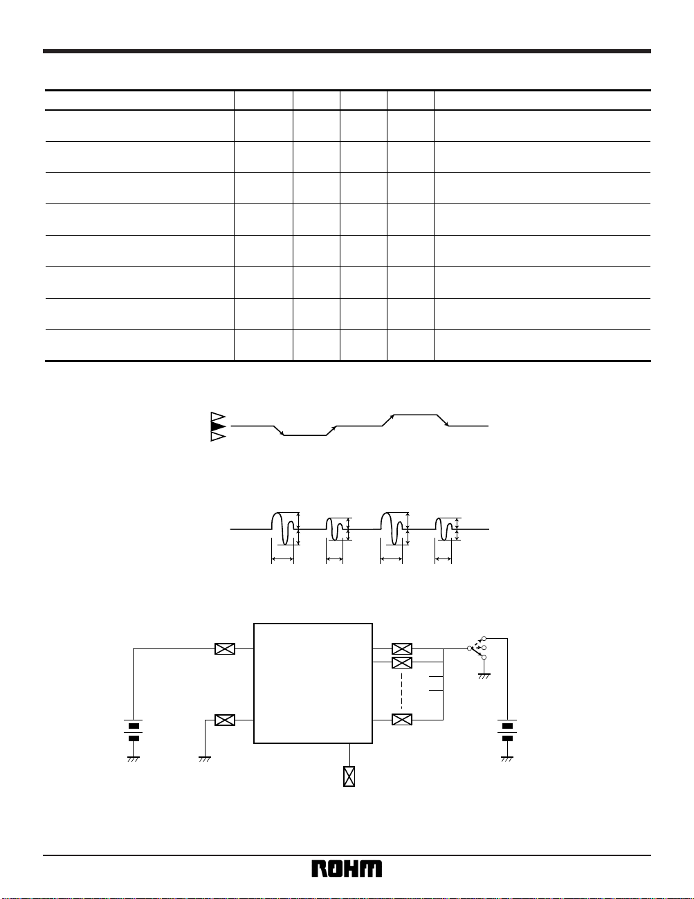
Transient characteristics (unless otherwise noted, Ta = 25°C)
Parameter Symbol Min. Max. Unit Conditions
Load Transient Voltage
2.85V→GND
– 100 100 mV
Load Transient 1 / 10 decay Time
2.85V→GND
τ
TD1 — 100 µs
Load Transient Voltage
GND→2.85V
– 100 100 mV
Load Transient 1 / 10 decay Time
GND→2.85V
τ
TD2 — 100 µs
Load Transient Voltage
2.85V→V
DD1
– 100 100 mV
Load Transient Voltage
2.85V→V
DD1
τTS1 — 100 µs
Load Transient Voltage
V
DD1→2.85V
– 100 100 mV
Load Transient Voltage
V
DD1→2.85V
τ
TS2 — 100 µs
EN = DISABLE
∗
, 4.0 ⬉ VDD1 ⬉ 5.5V
EN = DISABLE
∗
, 4.0 ⬉ VDD1 ⬉ 5.5V
EN = DISABLE
∗
, 4.0 ⬉ VDD1 ⬉ 5.5V
EN = DISABLE
∗
, 4.0 ⬉ VDD1 ⬉ 5.5V
EN = DISABLE
∗
, 4.0 ⬉ VDD1 ⬉ 5.5V
EN = DISABLE
∗
, 4.0 ⬉ VDD1 ⬉ 5.5V
EN = DISABLE
∗
, 4.0 ⬉ VDD1 ⬉ 5.5V
EN = DISABLE
∗
, 4.0 ⬉ VDD1 ⬉ 5.5V
All SCSI Lines: 2.85V→GND Level
All SCSI Lines: 2.85V→GND Level
All SCSI Lines: GND→2.85V Level
All SCSI Lines: GND→2.85V Level
All SCSI Lines: V
DD1→2.85V Level
All SCSI Lines: V
DD1→2.85V Level
All SCSI Lines: 2.85V→V
DD1 Level
All SCSI Lines: 2.85V→V
DD1 Level
∆VM
TD1
∆VMTD2
∆VMTS1
∆VMTS2
∗
BH9595FP-Y: EN = VDD1, BH9596FP-Y: GND
The transient characteristics are guaranteed design values.
– 5.5V
– 2.85V
0 V
tτ = 50ns
τTD1 τTD2 τTS1 τTS1
SCSI
Line
Potential
V
DD1 Level
2.85V
GND Level
VM
∆
VM
TD1 ∆VMTS1
∆
VM
TD2 ∆VMTS2
SCSI
Active
Terminator
+
–
SCSI Line
#1
#18
Same Voltage
as V
DD1
VM
V
DD1
+
–
Fig. 1 Measurement of transient characteristics
Page 5

5
Mulimedia ICs BH9595FP-Y / BH9596FP-Y
•
Application example
SCSI
Active
Terminator
SCSI
Active
Terminator
System
Power
System
Power
TERMPWR Line
+
–
+
–
2.2µ 2.2µ
V
DD1 VDD1
SCSI Line
SCSI DATA LINES
SCSI Line
#1
#18
#18EN EN
#1
GND
GND
VM
VM
Fig. 2
Page 6

6
Mulimedia ICs BH9595FP-Y / BH9596FP-Y
HSOP25
BH9595FP-Y
BH9596FP-Y
7.8 ± 0.3
5.4 ± 0.2
2.75 ± 0.1
1.95 ± 0.1
25 14
1
13
0.11
1.9 ± 0.1
0.36 ± 0.1
0.3Min.
0.25 ± 0.1
13.6 ± 0.2
0.8
0.15
BH9595FP - Y BH9596FP - Y
L
LH
Mode
Disable
Enable
H
2.5
1.50
1.00
0.50
250 50 75 100 125 150 175
POWER DISSIPATION: P (W)
AMBIENT TEMPERATURE: Ta (°C)
1.45W
Duty64%
Fig. 3
∗
1
∗
2
∗
3
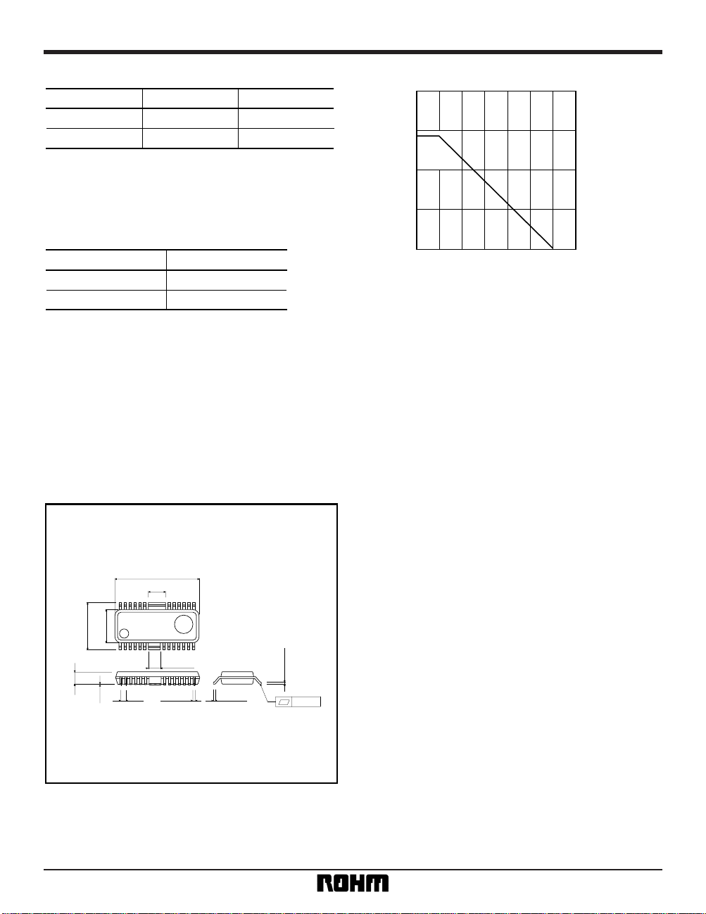
When mounted on a 90 × 50 × 1.6 (mm) glass epoxy board.
Reduced by 11.6mW for each increase in Ta of 1°C over 25°C.
Can withstand continuous use of 64% duty, at 25°C.
•
Mode selection table
Level
Normal
Shutdown
Conditions
“Low”
“High”
•
Thermal shutdown
(1) All outputs are opened at 175°C (typically).
(2) Temperature hysteresis is approximately 20°C.
(3) Thermal shutdown output table
•
Operation notes
(1) This terminator's operational range includes har-
monic frequencies. Mount to minimize ground
impedance.
(2) Connect the V
DD1 pin (TERMPWR) to a grounded
2.2µF bypass capacitor.
•
Thermal reduction curve
•
External dimensions (Units: mm)
 Loading...