

Page 1

1
Video ICs
VCR audio signal processing system
BH7775K
The BH7775K is an audio signal processing system IC that includes a peak-noise reduction (PNR) processor, an FM
modulator / demodulator circuit, an input / output switcher, an automatic FM detector circuit, an FM band-pass filter,
a normal-audio circuit, a regulator circuit, and automatic adjusting circuits (VCO and BPF).
•
Applications
VHS Video cassette recorders
•
Features
1) Operates off dual ± power supply which allows a
large reduction in the number of coupling capacitors
required. A built-in regulator makes it easy to construct a power supply system.
2) A built-in 2-wire serial control decoder circuit allows
serial control of the internal mode settings.
3) Automatic adjusting VCO and BPF circuits that use
the color signal subcarrier frequency (NTSC:
3.579545MHz and PAL: 4.433619MHz) ensure stable adjustment that is not effected by stress when
the chip is mounted, or variations over time.
4) 4-input switcher (turner, BS, and line 1 and 2).
Output switch with built-in STEREO / LEFT / RIGHT
switching, Hi-Fi / MIX / NORMAL switching, and BS
monitor functions.
5) The PNR processor and FM modulation / demodulation circuit provide reverse characteristics at record-
ing and playback. Also, carrier frequency adjustment
and FM de-emphasis / playback level adjustment
have been combined.
6) Built-in FM band-pass filter connects directly to the
playback amplifier and excels at attenuation of the
other channel. The FM recording output circuit has a
high-performance high-frequency cutoff filter that
produces a sine wave output.
7) Switching noise is reduced by a slope-control type
differential compensation circuit.
8) Built-in envelope detector circuit and noise-detecting
automatic FM detector circuit.
9) Built-in normal-audio signal processing circuit that
allows SP / LP / EP equalizer switching. Control terminal provided for use with the BA7755AF high-voltage head switcher.
Page 2

2
Video ICs BH7775K
•
Absolute maximum ratings (Ta = 25°C)
Parameter Symbol Limits Unit
V
CC
23, 55 pin · · · · · · · · · · 6.0
V
V
EE
59 pin · · · · · · · · · · · · – 6.0
V
V
IN 7, 8, 22 pin · · · · · · · · · 6.5 V
V
IN V
Pd mW
Topr – 10 ~ + 70 °C
Tstg – 55 ~ + 125 °C
Pin other than above
· · · · 6.0
Applied voltage
Power dissipation
Operating temperature
Storage temperature
∗
When IC is stand alone, reduced by 8.0mW for each increase in Ta of 1°C over 25°C. When mounted on a
90mm × 50mm, t = 1.6mm glass epoxy board, Pd = 1.3W (reduced by 13.0mW for each increase in Ta of
1°C over 25°C).
䊊
Not designed for rediation resistance.
800
∗
•
Recommended operating conditions (Ta = 25°C)
Power supply voltage
Power supply voltage
∗
The built-in regulator in this IC outputs + 5.0V from pin 55, and - 5.0V from pin 59. The supply voltage range
given above is the voltage to be applied to UNREG V
CC and UNREG VEE pins in the measurement circuit to
obtain regulator output. Therefore, the upper limit of the voltage range is set by the externally connected
transistor that forms the regulator circuit, and not by the IC itself. Note, also, that the lower limit will change
depending on the value of the resistor connected between the collector and base of the transistor.
Parameter
UNREG-V
CC
V
+ 7.0 ~
∗
UNREG-VEE V
+ 7.0 ~
∗
Symbol Range Unit
Page 3
3
Video ICs BH7775K
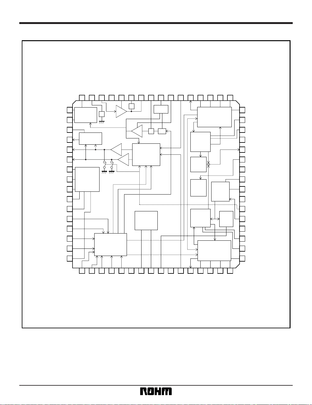
•
Block diagram
17
18
19
20
21
22
23
24
25
26
27
28
29
30
31
32
DC FB L
VCO f
0 ADJ L
DAC BF OUT L
GNML
FM PB IN
MUTE CTRL
VCB
BPF f
0 ADJ
FM ALC
RHS CTRL
AUDIO HEAD SW
PULSE IN
FM REC OUT
GNMR
DAC BF OUT R
VCO f0 ADJ R
DC FB R
NA REC OUT
HEAD EQ
NA HEAD IN
GNN
NA PB NFB
PB EQ
NA PB OUT
NA PB IN
NA ALC
NA FB
Hi-Fi IN R
Hi-Fi OUT R
NR TC R
WTNG1 R
WTNG2 R
NR EMPH R
BS R IN
BS L IN
TUNER R IN
TUNER L IN
TUNER M IN
GNDD
DATA
CLOCK
ENVE OUT / ADJ FLAG
/ Hi-Fi DET
FSC IN
Hi-Fi IN L
Hi-Fi OUT L
NR TC L
WTNG1 L
WTNG2 L
NR EMPH L
VREFP
LINE2 L IN
LINE2 R IN
LINE1 L IN
LINE1 R IN
V
EE
ERM
GND
ERP
Vcc
LINE OUT L
LINE OUT R
MIX OUT
MIX ALC
NA REC FB
REC EQ
64
63
62
61
60
59
58
57
56
55
54
53
52
51
50
49
12345678910111213141516
48 47 46 45 44 43 42 41 40 39 38 37 36 35 34 33
RECAMP
REC EQ
EQ
EQ
PB
MIX
AMP
AMP
OUTPUT
SWITCH
SW
ATT
LINE
AMP
LINE
AMP
REC
INPUT
SWITCH
DATA
DECODER
PNR
MODEM
ENVE
LOPE
FM BPF
D.O.
COM.
Hi-Fi
DET
MODEM
PNR
ALC
Page 4

4
Video ICs BH7775K
•
Pin descriptions
I / O circuitPin voltagePin name Function
3kΩ (2.5V Min.)
BS input (L and R).
TUNER input (L, R, and M).
Serial control GND.
Serial control data input.
Serial control clock input.
FM input Lch signal component envelope output.
Hi
-Fi DET output for FM input. ADJ FLAG output for ADJ.
fsc input terminal for VCO and BPF adjustment.
Hi
-Fi input for output switcher.
PNR audio output.
PNR attack and recovery time setting. Attack
R: 530
Ω, recovery R: 6.5kΩ.
Waiting characteristic low-frequency time constant setting
Waiting characteristic high-frequency time constant setting
NR emphasis time constant setting.
(external C = 0.01
µF)
PNR operating reference potential.
VCO control current setting terminal.
VCO control DAC voltage output terminal .
PNR, MODEM and BPF GND. L and R unconnected.
FM BPF center frequency adjustment.
FM ALC time constant setting.
Note) I / O circuit; EF: emitter follower, P-P: push pull, B: base, and C: collector.
All numerical values are standardized values.
Playback FM input. 660mVP-P Typ.
No input coupling capacitor (GND to V
CC).
Line output mute control input.
MODEM and BPF V
CC.
High-voltage head switch (BA7755) control terminal.
Audio head switching pulse input.
EE: recording FM output. Sine wave output.
PB: BPF output monitor terminal.
Pin No.
2, 1 BS IN L, R 0.0V 69.8kΩ
4, 3, 5 TUNER IN L, R, M 0.0V 47.0kΩ
6 GNDD 0.0V —
7 DATA IN — B (PNP)
8 CLOCK IN — B (PNP)
10 FSC IN 0.0V 200kΩ
11, 38 Hi-Fi IN L, R 0.0V 47kΩ
12, 37 Hi-Fi OUT L, R 0.0V EF: (P-P)
14, 35 WTNG1 L, R 0.0V 10kΩ
15, 34 WTNG2 L, R 0.0V 1.1kΩ
17, 32 DC FB L, R 0.0V 11.5kΩ
18, 31 VCO f
0 ADJ L, R 2.5V EF (NPN)
19, 30 VCO DAC BF OUT L, R 1.4V EF (NPN)
22 MUTE CTRL —
23 VCB 5.0V —
26 RHS CTRL — C (NPN)
24 BPF f
0 ADJ 1.9V EF (NPN) ~ 200Ω
27 AHSWP IN — B (PNP)
28 FM REC OUT
EE: 3.3V
PB: 3.3V
EF (NPN) ~ 200Ω
9
ENVE OUT / Hi-Fi DET
/ ADJ FLAG
EE: 0.8V
PB: 1.0V
EE: 50kΩ
PB, ADJ: EF (NPN)
13, 36 NR TC L, R – 5.0V —
16, 33 NR EMPH L, R 0.0V —
20, 29 GND (GNM) L, R 0.0V —
21 FM PB IN 0.0V 50kΩ
25 FM ALC 0.0V EF (NPN) ~ 2.5kΩ
Pin function - 1 / 2
Page 5

5
Video ICs BH7775K
∗
I / O circuit; EF: emitter follower, P-P: push pull, B: base, and C: collector.
All numerical values are standardized values.
Pin name Function Pin voltage
Normal line amplifier feedback.
Normal line amplifier ALC time constant setting
(attack and recovery time).
Normal line amplifier playback input.
Normal PB amplifier output.
Normal PB amplifier equalizer switch.
Normal PB amplifier feedback.
Normal audio GND.
Normal audio playback input.
Head resonance equalizer switch terminal.
Normal REC amplifier output.
Recording equalizer setting resistor terminal.
Normal REC amplifier feedback terminal.
ALC time constant setting for mixer amplifier
(attack and recovery time).
Mixer amplifier output for RF converter.
Line output
V
CC regulator.
V
CC regulator error output.
Output switch, regulator GND.
V
EE regulator error output.
VEE regulator
LINE 1 input (L and R).
LINE 2 input (L and R).
V
CC / 2 reference voltage. With power on detect
and precharge function.
I / O circuit
Pin No.
39 NA FB 0.0V 800Ω
41 NA PB IN 0.0V 105.2kΩ
42 NA PB OUT 0.0V EF (P-P) ~ 50Ω
43 PB EQ 0.0V OPEN / 25Ω
44 NA PB NFB 0.0V B (NPN)
45 GNN 0.0V —
47 HEAD EQ 0.0V 300kΩ / 29Ω
48 NA REC OUT 0.0V EF: (P-P)
49 REC EQ 0.0V 1kΩ
50 NA REC FB 0.0V B (NPN)
52 MIX OUT 0.0V EF (NPN)
54, 53 LINE OUT L, R 0.0V 330Ω
55 V
CC 5.0V —
56 ERP 5.0V C (NPN)
57 GND 0.0V —
58 ERM – 5.0V
– 5.0V
C (PNP)
59 V
EE —
61, 60 LINE1 IN L, R 0.0V 90.2kΩ
63, 61 LINE2 IN L, R 0.0V 90.2kΩ
64 VREFP
2.5V
10kΩ
40
NA ALC 0.0V EF (NPN) ~ 500Ω
46
NA HEAD IN 0.0V
REC: B (NPN)
REC: EF (P-P)
51
MIX ALC – 5.0V EF (NPN) ~ 500Ω
Pin function - 2 / 2
Page 6

6
Video ICs BH7775K
•
Input / Output circuits
Equivalent circuits for the control and input / output circuits - (1)
4 61
47k
– 2.0V
2.0V
[3, 5pin]
Vcc
V
EE
GND
Vcc
V
EE
GND
[60, 63,
62pin]
60.2k
30k
2.0V
– 2.0V
2
54
Vcc
V
EE
GND
Vcc
V
EE
GND
[1pin]
22.8k
47k
2.0V
– 2.0V
330
10.13k
25k
26k
30k
50
50
[53pin]
28
52
Vcc
V
EE
GND
Vcc
V
EE
GND
200
200
5p
8k
5k
200
200
47k
TUNER L, R, M (4, 3, 5pin)
BS L, R (2, 1pin)
MIX OUT (52pin)
LINE1 L / R, LINE2 L / R (61, 60, 63, 62pin)
LINE OUT (54, 53pin)
FM REC OUT (28pin)
Page 7

7
Video ICs BH7775K
Equivalent circuits for the control and input / output circuits - (2)
FM PB IN (21pin)
NA PB OUT (42pin)
NR REC OUT (48pin), NA REC NFB (50pin)
NA PB IN (41pin)
NA PB NFB (44pin), NA HEAD IN (46pin)
21
41
Vcc
V
EE
GND
Vcc
V
EE
GND
3.5V
50k
12.5k
20p 2k
100k
EEPB
30k
75.2k
PB
42
44
46
Vcc
V
EE
GND
100k
200
200
50
Vcc
V
EE
50
48
Vcc
V
EE
GND
200
200
50k
39k
10k
SP: ON
Page 8

8
Video ICs BH7775K
Equivalent circuits for the control and input / output circuits - (3)
AUDIO HEAD SWITCH PULSE IN (27pin)
RHS CTRL (26pin)
DATA (7pin), CLOCK (8pin) FSC IN (10pin)
ENVELOPE / Hi-Fi DET OUT (9 pin)
MUTE CTRL (22pin)
27
9
Vcc
V
EE
GND
Vcc
V
EE
GND
5k
30k 30k
PB
200
50k
26
22
Vcc
V
EE
GND
Vcc
V
EE
GND
5k
51k
16k
10k
3k
50k
10k
200
2.5V
8
10
Vcc
V
EE
Vcc
V
EE
GND
3V
10k
[7pin]
50k
200k
2k
Page 9

9
Video ICs BH7775K
•
Electrical characteristics
• Unless otherwise noted, the following measurement conditions apply:
UNREG – V
CC = + 10V
UNREG – V
EE = – 10V
Ta = 25°C
∗ With regard to the control voltages, refer to the mode holding voltage range given in p.141.
Output switch control (W1 bit 4, W1 bit 3 and W1 bit 2) STEREO
BS Through control (W1 bit 1) : OFF
LINE AMP gain (W3 bit 4 and W3 bit 3) : Standard ( + 10.6dB)
FM output control (W2 bit 5) : FM output on
FM OUT switch control (W2 bit 4, W2 bit 3 and W2 bit 2) : FM REC output MIX ration ( – 10.0dB)
NTSC / PAL control (W2 bit 0) : NTSC
Recording MUTE (W2 bit 1) : Recording MUTE
SP / EP control (W1 bit 5) : SP
FM detector level control (W4 bit 7, W4 bit 6) : Standard
ENVE characteristic control (W4 bit 5, W4 bit 4) : FNORM detector, no ENVE output
MUTE CTRL (pin 22) : L (MUTE)
LINE MUTE (W1 bit 0) : L (MUTE)
MODEM carrier frequency NTSC L channel 1.30MHz, PAL Lch 1.40MHz
MODEM carrier frequency NTSC R channel 1.70MHz, PAL Rch1.80MHz
Color signal subcarrier frequency NTSC 3.579545MHz, PAL 4.433619MHz
Signal frequency f = 1kHz
• Input condition 1 TU input V
IN = – 20.0dBV, LINE1 / LINE2 input VIN = – 10.0dBV, BS input VIN = – 16.0dB
• Input condition 2 TU input V
IN = – 10.6dBV, LINE1 / LINE2 input VIN = – 0.6dBV, BS input VIN = – 6.6dB
• Input condition 3 TU input V
IN = – 15.0dBV, LINE1 / LINE2 input VIN = – 5.0dBV, BS input VIN = – 11.0dB
• Input condition 4 TU input V
IN = – 5.0dBV, LINE1 / LINE2 input VIN = + 5.0dBV, BS input VIN = – 1.0dB
∗ 1 B.W. = 0.4 to 30kHz ∗ 2 DIN AUDIO
∗ Refer to Fig. 1 for the measurement circuit.
Regulator input voltage (–)
Parameter Symbol Min. Typ. Max. Unit Conditions
I
qp EE 29.0 38.6 51.3 mA
Iqp PB 40.3 53.7 71.4 mA
IqM EE – 22.1 – 16.6 – 12.5 mA
IqM PB – 23.9 – 18.0 – 13.5 mA
[REGULATOR]
V
CC
4.69 5.39
V
5.04
V
EE – 5.37 – 4.67 V– 5.02
EE mode, no input, after carrier
frequency adjustment.
Regulator input voltage (+)
Quiescent Current
(positive supply) EE
Quiescent Current
(positive supply) PB
Quiescent Current
(negative supply) EE
Quiescent Current
(negative supply) PB
PB mode, no input, FNORM, BPF,
after carrier frequency adjustment.
EE mode, no input, after carrier
frequency adjustment.
PB mode, no input, FNORM, BPF,
after carrier frequency adjustment.
Page 10

10
Video ICs BH7775K
∆VMODE — 8.0 22 mV
V
OMIX – 10.6 – 9.4 – 8.2 dBV
THD
MIX — 0.08 0.50 %
V
OBS – 10.5 – 8.1 dBV– 9.3
THD
BS — 0.08 %0.006
V
ONBS — – 86.0 dBV– 96.0
V
OLINE1 + 10.0 + 11.2 dB+ 10.6
V
OLINE2 + 11.2 + 12.4 dB+ 11.8
V
OLINE3 + 13.1 + 14.3 dB+ 13.7
V
ALCMIX – 4.4 – 1.4 dBV– 2.9
VIN = – 16.0dBV
VIN = – 16.0dBV,
∗
1
V
IN = – 20.0dBV
V
IN = – 20.0dBV
V
IN = – 20.0dBV
Input condition 1, simultaneous L & R input
Input condition 1, simultaneous L & R input
∗
1
Input condition 2, simultaneous L & R input
∗
2
, Connect BS IN to GND.
[LINE AMP] (INPUT: Hi-Fi IN L / R OUTPUT: LINE OUT L / R)
Input condition 1
Input condition 1,
∗
1
Rg = 1kΩ,
∗
2
Input condition 4
Input condition 4,
∗
1
Input condition 1
Input condition 1,
∗
1
THD = 1%,
∗
1
, ALC OFF
Input condition 2,
∗
2
, EE MODE, ALC OFF
[NORMAL REC AMP]
MT
RECN — – 94.0 – 70.0 dBV
(INPUT: TU IN M, TU IN L / R, LINE1 IN L / R, LINE2 IN L / R, BS IN L / R OUTPUT: NA REC OUT)
V
OEE – 11.6 – 9.2 dBV– 10.4
THD
EEN — 0.10 %0.039
V
ONEEN — – 71.3 dBV
– 81.5
V
ALCN1 – 8.9 – 5.9 dBV– 7.4
THD
ALCN —
0.15
%
0.045
V
ORECN – 9.6 –6.6 dBV– 8.1
THD
RECN — 0.20 %0.079
V
OMRCN 7.0 — dBV9.2
(INPUT: TU IN L / R, LINE1 IN L / R, LINE2 IN L / R, BS IN L / R OUTPUT: MIX OUT)
[MIX AMP]
(INPUT: TU IN M, TU IN L / R, LINE1 IN L / R, LINE2 IN L / R, BS IN L / R OUTPUT: LINE OUT L / R)
[NORMAL EE THROUGH]
Parameter Symbol Min. Typ. Max. Unit Conditions
CTEE
——
– 75.0 dBV
[Hi-Fi EE THROUGH]
〈MANUAL MODE〉
V
OEE – 10.6 – 8.2 dBV– 9.4
CB
EE – 0.8 0.8 dB0.0
THD
EE — 0.10 %0.017
V
OMEE 9.0 — dBV10.7
V
ONEE — – 86.0 dBV– 93.0
MTEE
— – 95 dBV– 105
Input condition 1
Input condition 1
Input condition 1
∗
1
THD = 1%,
∗
1
Relevant input shorted to GND,
∗
2
Input condition 2
∗
2
(LINE OUT)
ST / L / R / N, MIX ON / OFF
Mode switching operating point voltage difference.
(INPUT: TU IN L / R, LINE1 IN L / R , LINE2 IN L / R, BS IN L / R OUTPUT: LINE OUT L / R)
Relevant input: shorted to GND
Non-relevant input: Input condition2,
∗
2
Switching DC offset
Line output level
Channel balance (L / R)
Distortion
Maximum output level
Output residual noise
Crosstalk
Muting level
Output level
Distortion
Output residual noise
Line amplifier gain 1
Line amplifier gain 2
Line amplifier gain 3
Output level
Distortion
MIX ALC level
Output voltage level
Distortion
Output residual noise
ALC level 1
ALC distortion
Output voltage level
Distortion
Maximum output level
Output level for EE
[BS THROUGH] (INPUT: BS IN L / R OUTPUT: LINE OUT L / R)
Page 11

11
Video ICs BH7775K
[NORMAL PB AMP] (INPUT: NA HEAD IN, OUTPUT: LINE OUT)
[EQ SWITCH]
[PNR ENCODE MODE]
[PNR DECODE MODE]
Encode output level
Compression characteristic
Encode distortion
Output residual noise
Output voltage level
Expansion characteristic
Time constant setting resistor
Output voltage level
Distortion
Output residual noise
Open loop gain
(PB PRE AMP)
REC FB resistance SP
REC FB resistance EP
REC EQ resistance
PB EQ SW impedance
HEAD EQ SW impedance
RHS control current
RHS control leakage current
[RHS CONTROL]
G
VPBNOR
VOPSN
THDPBN
VONPBN
RREC SP
RREC SP
RREC EQ
REQ PB
REQ HEAD
IIN RHS
IL RHS
CMP
EXP
R
DET
THDEND
VONEC
VODEC
VOENC
58.0
– 13.4
—
—
8.3
40.7
0.83
—
—
98
—
– 26.4
– 52.4
5.10
—
—
– 11.2
– 17.0
66.7
– 11.6
0.19
– 63.6
10.0
49.0
1.00
25
29
118
—
– 24.7
– 50.2
6.15
0.17
– 56.5
– 9.4
– 15.7
—
– 9.8
0.40
– 55.0
11.7
57.3
1.17
50
50
140
1
– 23.0
– 48.0
7.20
0.37
– 51.5
– 7.6
– 14.4
dB
dB
%
dBV
kΩ
kΩ
kΩ
Ω
Ω
µA
µA
dB
dB
kΩ
%
dBV
dBV
dBV
V
IN = – 15.7dBV
Input condition 1
TU input V
IN = – 20dBV→ – 70dBV
output level difference.
Input condition 1,
∗
1
Connect the pertinent input to GND,
∗
2
VIN = – 15.7dBV→ – 40.7dBV
output level difference.
Resistance value connected between pins 13 and
36 and VEE. (when VCCS and VEES applied)
VIN = – 70dBV
OUTPUT: NA PB OUT
V
IN = – 70dBV
V
IN = – 70dBV,
∗
1
Rg = 1k Ω,
∗
2
SP MODE
EP MODE
SP MODE
EP MODE
Resistor connected between pin 49 and GND.
Parameter Symbol Min. Typ. Max. Unit Conditions
Page 12

12
Video ICs BH7775K
PB mode: Input FM PB IN = 660mV
P-P
, f = 1.30MHz, 1.70MHz 1: 1 MIX, after BPF center frequency adjustment. Inpu
DEV = DEV
L,R
(frequency deviation given above). EE / PB line out level difference.
EE mode: VIN = – 10.0dBV after carrier
frequency adjustment.
Demedulation output
level
Demedulation output
level 2
Demedulation distortion
Demedulation SW
noise level
Demedulation noise
level
Line output recording /
playback level
difference
DEVL = ± 50.0kHz, f = 10kHz
DEV
R = ± 50.0kHz, f = 10kHz
DEV
L = ± 50.0kHz, f = 1kHz
DEV
R = ± 50.0kHz, f = 1kHz
DEV
L = ± 50.0kHz, f = 1kHz,
∗
1
DEV
R = ± 50.0kHz, f = 1kHz,
∗
1
f = 10kHz, AUDIO H. SW. P = – Hz
5V
P-P rectangular-waveform input. After
10kHz TRAP passes DEV. = ± 25.0kHz
∗
2
Unmodulated
∗
2
Parameter Symbol Min. Typ. Max. Unit Conditions
V
ODL2
VODR2
VODR VODR
VODR
– 5.0
dBV
V
ODL VODL VODL
– 5.0
dBV
(INPUT: TUNER IN L / R, LINE1 IN L / R, LINE2 IN L / R, BS IN L / R, OUTPUT: FM REC OUT L / R)
V
RPR – 1.2 + 1.2 dB
0.0
V
RPL
Rch
Lch – 1.2 + 1.2 dB
0.0
f
NOLLch 1.2950 1.3050 MHz
1.3000
f
NORRch 1.6950 1.7050 MHz
1.7000
f
POLLch 1.3945 1.4055 MHz
1.4000
f
PORRch 1.7935 1.8045 MHz
1.7990
DEVL 45.5 57.5 ± kHz
51.5
DEV
R 45.0 57.0 ± kHz
51.0
DEV
Max.L 116 160 ± kHz
138
DEV
Max.R 116 160 ± kHz
138
VOFML 320 420 mVP-P
365
VOFMR
Lch
Rch
Lch
Rch
Lch
Rch 325 425 mV
P-P
370
f
2L — – 40.0 dB
– 53.0
f
2R — – 40.0 dB
– 48.0
f
3L — –40.0 dB
– 52.0
f
3R
Lch
Rch
Lch
Rch — –42.0 dB
– 55.0
f
LR – 12.0 – 8.4 dB
– 10.2
V
ODL – 11.5 – 7.1 dBV
– 9.3
V
ODR – 11.5 – 7.1 dBV
– 9.3
THD
DL — 0.35 %
0.12
THD
DR
Lch
Rch
Lch
Rch
Lch
Rch — 0.35 %
0.13
V
ODSWL — — dBV
—
V
ODSWR — — dBV
—
V
ONDL — – 85.0 dBV
– 95.0
V
ONDR
Lch
Rch
Lch
Rch — – 85.0 dBV
– 95.0
Carrier frequency
NTSC
Carrier frequency
PAL
Frequency deviation
Maximum frequency
deviation
FM output level
Carrier 2nd harmonic
Carrier 3rd harmonic
FM MIX ratio (FM MIX1 mode)
No input, V
CC
stable, after automatic adjustment
f
SC =
3.579545MHz
V
IN =
150 ~ 500mV
P-P
No input, VCC stable, after automatic adjustment
f
SC =
4.433619MHz
V
IN =
150 ~ 500mV
P-P
FM OUT SW: FM L mode
FM OUT SW: FM R mode
2nd stage harmonics and fundamental harmonics
spectral ratio Lch: FM L mode, Rch: FM R mode
3rd stage harmonics and fundamental harmonics
spectral ratio Lch: FM L mode, Rch: FM R mode
Input condition 1
Input condition 4 (f
=
10kHz)
1.3MHz / 1.7MHz spectrum ratio.
[MODEM REC MODE]
[MODEM PB MODE] (INPUT: FM PB IN, OUTPUT: LINE OUT L / R)
Carrier frequency, after BPF fo adjustment, V
IN = 660mVP-P, 1.30MHz, 1.70MHz MIX IN
[Recording→ playback total characteristics] (EE · · · INPUT: LINE IN L / R, OUTPUT: LINE OUT L / R)
(PB · · · INPUT: FM PB IN, OUTPUT: LINE OUT L / R)
– 10.0
– 10.0
– 7.5
– 7.5
Page 13

13
Video ICs BH7775K
ATTNL
1.15
ATT
NLC
– 9.5
ATTNLC
– 5.0
ATTNLC
– 2.0
dB
1.15MHz + 1.70MHz
ATT
NL
1.45
ATT
NLC
– 8.6
ATTNLC
– 5.0
ATTNLC
– 2.0
dB 1.45MHz + 1.70MHz
ATT
NL
1.70
——
ATT
NLC
– 30.0
dB
1.30MHz + 1.70MHz
f = 1.505MHz, V
IN = 200mVP-P
∆VBPFN – 5.0 5.0 dB
0.0
f = 1.605MHz, V
IN = 200mVP-P
∆VBPFP – 5.0 5.0 dB
0.0
〈NTSC Lch〉
1.30MHz + 1.70MHz
ATT
NLC – 14.2 – 8.1 dB
– 11.1
ATT
NR
1.55
ATT
NRC
– 8.3
ATTNRC
– 4.7
ATTNRC
– 1.9
dB
1.55MHz + 1.30MHz
ATT
NR
1.85
ATT
NRC
– 10.6
ATTNRC
– 5.4
ATTNRC
– 1.6
dB 1.85MHz + 1.30MHz
ATT
NR
1.30
——
ATT
NRC
– 30.0
dB
1.30MHz + 1.70MHz
〈NTSC Rch〉
1.30MHz + 1.70MHz
ATTNRC – 15.5 – 9.3 dB
– 12.3
ATT
PL
1.25
—
ATT
PLC
– 5.0
—
dB
1.25MHz + 1.80MHz
ATT
PL
1.55
—
ATT
PLC
– 5.2
—
dB 1.55MHz + 1.80MHz
ATT
PL
1.80
——
ATT
PLC
– 30.0
dB
1.40MHz + 1.80MHz
〈PAL Lch〉
1.40MHz + 1.80MHz
ATTPLC – 1.28 – 6.7 dB
– 9.7
ATT
PR
1.65
—
ATT
PRC
– 4.6
—
dB
1.65MHz + 1.40MHz
ATT
PR
1.95
—
ATT
PRC
– 5.3
—
dB 1.95MHz + 1.40MHz
ATT
PR
1.40
——
ATT
PRC
– 30.0
dB
1.40MHz + 1.80MHz
〈PAL Rch〉
1.40MHz + 1.80MHz
ATTPRC – 14.8 – 8.6 dB
– 11.6
[FM BPF] (INPUT: FMPB IN, OUTPUT: BPF MONITOR L / R) V
CC stable, after automatic adjustment
BPF L / R level difference NTSC
BPF L / R level difference PAL
1.30MHz insertion loss
1.15MHz attenuation
1.45MHz attenuation
1.85MHz attenuation
1.30MHz attenuation
1.40MHz insertion loss
1.25MHz attenuation
1.55MHz attenuation
〈LcH, RcH mix input signal〉 660mV
P-P (RATIO 1: 1), FM ALC ON
1.70MHz attenuation
1.70MHz insertion loss
1.55MHz attenuation
1.80MHz attenuation
1.80MHz insertion loss
1.65MHz attenuation
1.95MHz attenuation
1.40MHz attenuation
Parameter Symbol Min. Typ. Max. Unit Conditions
Page 14

14
Video ICs BH7775K
Parameter Symbol Min. Typ. Max. Unit Conditions
V
DDO 77.0 83.0 89.0 dBµ
τ
FNDLY 110 125 140 ms
V
THHOLD 1.66 2.66 3.66 V
V
ENVSP0 — 100 mV0
V
ENVSP1 2.22 3.22 V2.72
V
ENVSP2 3.70 4.20 V3.95
V
ENVEP1 2.18 3.18 V2.68
V
HDETL — 100 mV0
V
HDETH 3.50 — V4.00
∆τ
HOLD 6.47 9.07 µs7.77
[DO detect circuit]
[FNORM to Hi-Fi return delay circuit]
[Hold pulse circuit]
Envelope output level SP0
Envelope output level SP1
Envelope output level SP2
Envelope output level EP1
Hi-Fi DET output DC FNORMAL
Hi-Fi DET output DC HiFi
FM PB IN (1.3MHz, 1.7MHz, 1: 1 MIX)
time from 660mV
P-P input to ENVE OUT
rise. Audio head pulse in: f = 30Hz,
5V
P-P rectangular waveform.
V
IN = 0dB, SP MODE
V
IN = + 10dB, SP MODE
V
IN = – 4dB, EP MODE
V
IN = 0dB
[Envelope output circuit] (INPUT: FM PB IN, OUTPUT: ENVE OUT)
0dB = 660mV
P-P, 1.3MHz & 1.7MHz MIX IN
〈CLOCK IN〉
V
H8L 0.0 0.5 V—
V
H8H 2.5 VCC V—
〈DATA IN〉
V
H7L 0.0 0.5 V—
V
H7H 2.5 VCC V—
MUTE CTRL
V
H22L 0.0 1.0 V—
V
H22H 3.9 VCC V—
L mode holding voltage
H mode holding voltage
L mode holding voltage
H mode holding voltage
MUTE holding voltage
DC MUTE holding voltage
[Voltage for preserving the control system mode]
No signal, SP MODE
Hysteresis (0.5V)
No signal
Input level to give DO due to attenuation.DO detector level
Return delay time
Audio head switch pulse
threshold voltage
Hold pulse width
Page 15

15
Video ICs BH7775K
•
Measurement circuit
A
V
V
A
A
A
V
V
V
17
18
19
20
21
22
23
24
25
26
27
28
29
30
31
32
33µ
0.01µ
0.022µ
33µ
0.01µ
0.022µ
4.7µ
3.3µ
47k
V
EE
Hi-FiINL
ENVEOUT/ADJFLAG
Hi-FiDET
10k
MUTE CTRL
FM PB IN
50
10k
25.3k
47k
27k
AUDIO
HEAD SWITCH PULSE IN
FM REC OUT
27k
47k
64
4.7µ
100µ
100µ
1500p
V
EE
VEE
UNREG VEE
VEE
1200p
NAME COUI
NAME AOIN
330k
0.01µ
0.1µ
100µ
33µ
3.3µ
10µ
V
EE
4.7µ
0.01µ
0.022µ
V
EE
1M
330
22µ
12k
0.2k
500
1k
0.01µ
UNREG V
CC
VCC
LINE OUT L
LINE OUT R
MIX OUT
63
62
61
60
59
58
57
56
55
54
53
52
51
50
49
12345678910111213141516
48 47 46 45 44 43 42 41 40 39 38 37 36 35 34 33
RECAMP
REC EQ
EQ
EQ
PB
MIX
AMP
AMP
OUTPUT
SWITCH
SW
ATT
LINE
AMP
LINE
AMP
REC
INPUT
SWITCH
DATA
DECODER
PNR
MODEM
ENVE
LOPE
FM BPF
D.O.
COM.
Hi-Fi
DET
MODEM
PNR
ALC
1k
FSCIN
CLOCK
DATA
TUNER M IN
1k
1k
1k
1k
1k
1k
1k
1k
1k
4.7k
4.7k
4.7k
4.7k
4.7k
4.7k
4.7k
4.7k
4.7k
4.7k
4.7k
22k
1500p
22k
22k
2.2M
47µ
TUNER L IN
TUNER R IN
BS L IN
BS R IN
LINE2 L IN
LINE2 R IN
LINE1 L IN
LINE1 R IN
22k
10µ
500
Fig.1
Page 16

16
Video ICs BH7775K
•
Application example
BIAS
OSC
17
18
19
20
21
22
23
24
25
26
27
28
29
30
31
32
33µ
0.022µ
33µ
0.01µ
0.022µ
4.7µ
3.3µ
VEE
ENVELOPE/Hi-Fi DET OUT/ADJ FLAG
MUTE CTRL
FM PB IN
25.3k
47k
27k
AUDIO HEAD SWITCH PULSE IN
P/R CTRL
FM REC OUT
27k
47k
64
4.7µ
100µ
100µ
1500p
V
EE
UNREG VEE
VEE
1200p
0.1µ
100µ
3.3µ
10µ
V
EE
4.7µ 0.01µ
0.022µ
V
EE
1M
330
330k
12k
22µ
0.01µ
8.2k
0.01µ
UNREG V
CC
VCC
LINE L OUT
LINE R OUT
MIX OUT
63
62
61
60
59
58
57
56
55
54
53
52
51
50
49
12345678910111213141516
48 47 46 45 44 43 42 41 40 39 38 37 36 35 34 33
RECAMP
REC EQ
EQ
EQ
PB
MIX
AMP
AMP
OUTPUT
SWITCH
SW ATT
LINE
AMP
LINE
AMP
REC
INPUT
SWITCH
DATA
DECODER
PNR
MODEM
ENVE
LOPE
FM BPF
D.O.
COM.
Hi-Fi
DET
MODEM
PNR
ALC
FSCIN
CLOCK
DATA
TUNER M IN
4.7k
4.7k
4.7k
4.7k
4.7k
4.7k
4.7k
4.7k 22k
1500p
2.2M
47µ
TUNER L IN
TUNER R IN
BS L IN
BS R IN
LINE2 L IN
LINE2 R IN
LINE1 L IN
LINE1 R IN
BA7755
1234
8765
33µ
10µ
Fig.2
Page 17

17
Video ICs BH7775K
•
Electrical characteristic curve
FREQUENCY: f (MHz)
GAIN: GV (dB)
Lchannel
Rchannel
0.75
0.90 1.05 1.20 1.35 1.5 1.65 1.80 1.95 2.10 2.25
– 45
– 55
– 50
– 35
– 40
– 25
– 15
– 5
– 30
– 20
– 10
Fig. 3 FM BPF frequency characteristics (NTSC)
•
External dimensions (Units: mm)
0.15 ± 0.1
48 33
32
17
49
64
1
16
14.0 ± 0.2
16.4 ± 0.3
14.0 ± 0.2
0.35 ± 0.1
0.05
0.5
16.4 ± 0.3
0.8
2.7 ± 0.1
0.15
QFP-A64
 Loading...