

Page 1
1
Multimedia ICs
Vocal fader IC with input selector
BH3810FS
The BH3810FS is a vocal fader IC that is serial control compatible. It has mode switching that also includes a voice
multiplexing mode, a five-input selector, a gain selector and other such features, which can all be controlled serially.
Eight open-collector terminals and two tri-state terminals are provided on the chip to facilitate control by other ICs.
•
Applications
Component stereo systems, CD radio cassette players, TVs and car stereos.
•
Features
•
Absolute maximum ratings (Ta = 25°C)
•
Recommended operating conditions (Ta = 25°C)
Parameter
Applied voltages
Power dissipation
Operating temperature
Storage temperature
V
DD
Pd
Topr
Tstg
+ 5.5
850
∗
– 40 ~ + 85
– 55 ~ + 125
V
VEE – 4.5
Symbol Limits Unit
mW
°C
°C
Maximum open collector voltage VOP 14 V
∗
Reduced by 8.5mW for each increase in Ta of 1°C over 25°C ,
when mounted on a 50mm × 50mm × 1.6mm board.
1) Built-in low-pass filter can perform vocal fader function (erasing of vocals from commercially available
music software) using just one chip.
2) Serial control can be used to switch between vocal
fader, through, multiplex, and mute modes.
3) Built-in gain selector allows selection of gain from
6dB to 20dB in 2dB steps.
4) Five-channel input selector.
5) Mic. mixing amplifier with mute function. Key controller input also provided.
6) SSOP-A32 pin package.
Parameter
Power supply voltage
V
DD 4.0 ~ 5.3 V
V
EE – 4.3 ~ – 3.0 V
Symbol Limits Unit
Page 2
2
Multimedia ICs BH3810FS
•
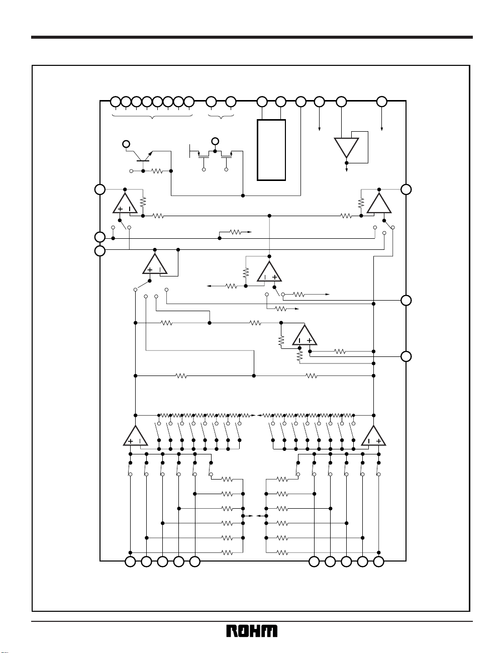
Block diagram
PORT124PORT223PORT322PORT421PORT520PORT619PORT718PORT817PORT916PORT1015SCK14SI13DGND12VDD
11
AGND
10
VEE
VDD
VEE
9
OUTPUT—L
8
MIC
—IN
7
LPF
6
TK
27
FK
26
OUTPUT—R
25
PORT1 ~ 8
7k
50k
50k
50k50k
50k50k
50k
50k
50k
50k
50k
50k
50k
50k
15k
10k
L
R
VF
50k
7k
7k
PORT9 ~ 10
DIGITAL CONTROL
V
DD
+
–
7k
+
–
30k
10k
10k
30k
20k
20k
6dB
(0dB)
8dB
(2dB)
10dB
(4dB)
12dB
(6dB)
14dB
(8dB)
16dB
(10dB)
18dB
(12dB)
20dB
(14dB)
20dB
(14dB)
18dB
(12dB)
16dB
(10dB)
14dB
(8dB)
12dB
(6dB)
10dB
(4dB)
8dB
(2dB)
6dB
(0dB)
—RA
32
—RB
31
—RC
30
—RD
29
INPUT
—RE
28
—LE
5
—LD
4
—LC
3
—LB
2
INPUT
—LA
1
Page 3
3
Multimedia ICs BH3810FS
•
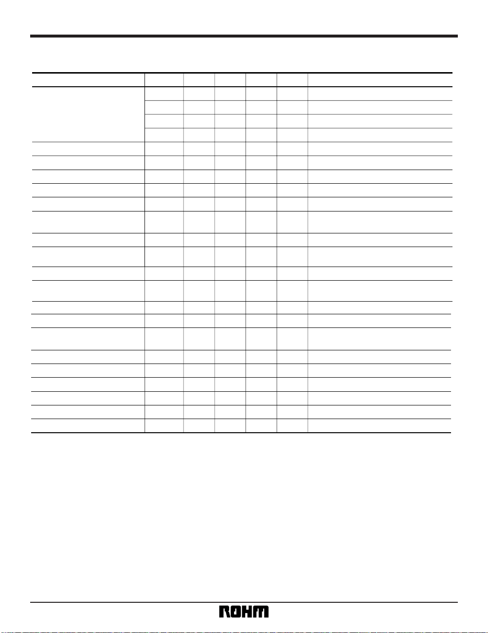
Electrical characteristics (unless otherwise notes, Ta = 25°C, VDD = 5V, VEE = – 4V, G = 14dB, f =1kHz,
Rg = 600Ω, V
IN = 150mV, and RL = 100kΩ)
Parameter
Quiescent current
Maximum output voltage
I
Q1
+
I
Q1
–
I
Q2
+
I
Q2
–
Vom
mA
Symbol
—
—
—
—
1.5
Min.
4.5
4.1
10.0
7.6
2.2
Typ.
10.0
10.0
20.0
20.0
—
V
rms
Max. Unit Conditions
mA
mA
mA
THD
=
1%, through mode
L, R gain
G
VT
11 14 17 dB Through mode
Low-frequency gain
G
VF
8 11 14 dB Vocal fader mode, f
=
100Hz
Microphone gain
G
VM
5 8 11 dB
Crosstalk
CT 54 64
—
dB f
=
1kHz, through mode
f
=
1kHz, mute mode or input mute
Mute attenuation
MU 60 80
—
dB
Vocal suppression ratio
SV 15 20
—
dB Vocal fader mode, f
=
1kHz
Total harmonic distortion
THD
—
0.004 0.05
%
VO =
1V
rms
, through mode, BW 400Hz
to 30kHz
Noise level
V
N
—
15 22
µ
V
rmsRg
=
0, DIN AUDIO
∗
Mode switch output DC
differential
∆
DCB
—
018mV
Between each mode with key controller on
Input impedance
R
IN
35 50 65 k
Ω
Pins 1 to 5, pins 26, pins 28
to
32
Input selector crosstalk
CT
IN
80
——
dB f
=
1kHz
"L" output voltage
V
OL
—
0.15 0.5 V Pins 17
to
27, IOL =
5mA
"H" output leakage current
I
OH
—
0 2.0
µ
A
Pins 17 to 24, 13V applied to collector
Tri-state "H" output voltage
V
SOH
4.5 4.85
—
V Pins 15 to 16, Io
=
1mA
Tri-state "L" output voltage
V
SOL
—
0.05 0.5 V Pins 15 to 16, Io
=
1mA
SI pin source current (pin 13)
I
SI
—
0.4 10
µ
A When SI pin is at DGND potential
SCK pin source current (pin 14)
I
SCK
—
0.2 10
µ
A When SCK pin is at DGND potential
Pins 17 to 24, 0.5V between PORT
terminal and GND voltage = 0.5V
Port output current
I
PMax.
5.0 12
—
mA
Through mode V
EE
current
Through mode V
DD
current
Through mode D9 to D16 data1
Through mode D9 to D16 data1
∗
Measured using a Matsushita VP-9690A (average value detector, effective value display) DIN AUDIO filter.
Operating specifications: same phase for the input and output signals.
䊊 Not designed for radiation resistance.
—
Page 4

4
Multimedia ICs BH3810FS
•
Measurement circuit
17
PORT
8
9
PORT
16
18
PORT
7
10
PORT
15
19
PORT
6
SCK
14
20
PORT
5
SI
13
21
PORT
4
DGND
12
22
PORT
3
VDD
11
23
PORT
2
AGND
10
24
PORT
1
VEE
9
25
OUTPUT
-R
-L
OUTPUT
8
26
FK
-IN
MIC
7
27
TK
LPF
6
28
-RE
-LE
5
29
-RD
-LD
4
30
-RC
-LC
3
31
-RB
-LB
2
32
INPUT
-RA
-LA
INPUT
1
A
V V V
A
V V V V V
V
1212
12
A
12
A
12
A
12
A
12
A
12
A
12
12
13V
0.1µF
1212121212
1
2S2
Rg = 600Ω
50k
1212
12
1212
12
S14S12S11S10S9S8
S13S7
12
S17
V
12
1
2
S18
S16
12
S22
1mA
1mA
V
DD
12
S21
S6S5
12
S20
S19
S4S3
VV
RL
100k
V
AA
12
S0
10k
10k
12
S1
AA
DATA
LATCH
CLOCK
THD
V
Fig. 1
Page 5

5
Multimedia ICs BH3810FS
•
Circuit operation
(1) About the data format
Data
Descri-
ption
D0 D1 D2 D3 D4 D5 D6 D7 D8 D9 D10 D11 D12 D13 D14 D15 D16 D17 D18 D19 D20 D21 D22
17pin 18pin 19pin 20pin 21pin 22pin 23pin 24pin 15pin 16pin
Input
selector
Input
selector
Mode
selector
Open collector port
Tri-state
port
Tri-state
port
Mic.
mute
Chip
select
3bit
Bit number
3bit 3bit 8bit 2bit 2bit 1bit 2bit
D23
MSB 24 bits total LSB
Fig.2
Data format
Pin
name
Data
0
1
1
(24pin)
PORT
D16
2
(23pin)
PORT
D15
3
(22pin)
PORT
D14
4
(21pin)
PORT
D13
5
(20pin)
PORT
D12
6
(19pin)
PORT
D11
7
(18pin)
PORT
D10
8
(17pin)
PORT
D9
Current sink OFF
Current sink ON
Output port: open collector
D22 D23
00
• Address is "00"
Mode selector
Gain selector
Mic
Key controller
Input selector
Through mode
6dB
Mute OFF
OFF
LA, RA
At power on
D19
PORT9 (16pin)
D19, D20
D20 Mode
LOW00
OPEN01
OPEN10
HI11
D17
PORT10 (15pin)
D17, D18
D18 Mode
LOW00
OPEN01
OPEN10
HI11
Tri-state
D21 Mode
Mic. ON0
Mic. MUTE1
Mic. mute
Output port: current attraction OFF
Tri-state port: Low
Page 6

6
Multimedia ICs BH3810FS
D0
0
Mode
MUTE
MUTE0
D1
0
0
D2
0
1
MUTE010
INPUT—LA, INPUT—RA011
INPUT—LB, INPUT—RB100
INPUT—LC, INPUT—RC101
INPUT—LD, INPUT—RD110
INPUT—LE, INPUT—RE111
Input selector 〈3 bits〉 D0 to D2
D3
0
0
D4
0
0
D5
0
1
010
011
100
101
110
Gain select
6dB
8dB
10dB
12dB
14dB
16dB
18dB
20dB111
Gain selector 〈3 bits〉 D3 to D5
The gain is the total gain from input to output.
D6
0
LOUT
MUTE
VOCALFADE0
D7
0
0
L01
L01
FK10
FK10
FK11
FK
ROUT
MUTE
VOCALFADE
L
R
FK
FK
FK
FK
TK Mode
MUTE
VOCALFADE
L
L
L + R
R
L
VOCALFADE Key controller, vocal fader
Key controller, L channel
Key controller, R channel
Key controller, L + R
Through
L channel
Vocal fader
Mute
11
D8
0
1
0
1
0
1
0
1
Mode selector 〈3 bits〉 D6 to D8
Page 7

7
Multimedia ICs BH3810FS
SCK
(clock signal)
SI
(DATA signal,
LATCH signal)
D22 D23
tw
90%
90%
90%
10%
10%
10%
tw
tsu th ts tw (LATCH)
tw (DATA)
∗
When LATCH is "H", the DATA signal is forced "L" internally.
∗
The read decision for the DATA signal (SI) is made by the signal when the CLOCK signal rises.
∗
The read decision for the LATCH signal (SI) is made by the signal when the LATCH signal itself rises.
∗
A "L" must follow at the end of each signal to wait for the next signal.
Fig.3
(2) Timing chart
Serial data timing (timing for the IC terminals)
•
Timing chart constants (Ta = 25°C, VDD = 5V and VEE = – 4V)
Parameter
H input voltage V
IH 4.0 5.0 6.0 V
M input voltage VIM 2.0 2.5 3.0 V
L input voltage VIL – 0.3 0 1.0 V
Minimum clock width tw 2.0 — — µs
Minimum data width tw (DATA)
tw (LATCH)
4.0 — — µs
Minimum latch width 2.0 — — µs
Setup time (DATA to CLK) tsu 1.0 — — µs
Hold time (CLK to DATA) th 1.0 — — µs
Setup time (DATA, CLK to LATCH)
ts 1.0 — — µs
Symbol Min. Typ. Max. Unit
∗
If the voltage between VDD and DGND changes, the values above will change.
Page 8

8
Multimedia ICs BH3810FS
17
PORT
8
9
PORT
16
18
PORT
7
10
PORT
15
19
PORT
6
SCK
14
20
PORT
5
SI
13
21
PORT
4
DGND
12
22
PORT
3
V
DD
11
23
PORT
2
AGND
10
24
PORT
1
V
EE
9
25
OUTPUT
-R
-L
OUTPUT
8
26
FK
-IN
MIC
7
27
TK
LPF
6
28
-RE
-LE
5
29
-RD
-LD
4
30
-RC
-LC
3
31
-RB
-LB
2
32
INPUT
-RA
-LA
INPUT
1
10k10k10k10k10k10k10k10k
POWER
AMP
GND
MICROPHONE
DATA
V
DDVEE
LATCH
10k
10k
µ—con
CLOCK
0.1µF
+
AUX
TAPE
TUNER
CD
MD
key—con
Fig. 4
•
Application circuit
Page 9

9
Multimedia ICs BH3810FS
•
Operation notes
(1) We guarantee the application circuit design, but recommend that you thoroughly check its characteristics in actual use.
If you change any of the external component values, check both the static and transient characteristics of the circuit,
and allow sufficient margin in your selections to take into account variations in the components and ICs.
Note that Rohm has not fully investigated patent rights regarding this product.
(2) The vocal fader function
The effect of the vocal fader is realized by negating the same-phase components. In the bass region, the first-stage
low-pass filter leaves the source sound as is, even for the same-phase components. Therefore, depending on the
music, the effect may be small.
(3) The low-pass filter that leaves the vocal fader bass
The low-pass filter is formed by connecting a capacitor to pin 6. A 20kΩ resistor (design value) and this capacitor set
the cutoff frequency.
The optional attenuation of the first-stage low-pass filter frequency is:
(4) AGND (pin 10) and DGND (pin 12)
AGND is the ground for the IC's internal analog circuits, and DGND is the ground for the internal ports 1 to 10.
Connect the two grounds externally.
(5) Switching noise
If you are troubled by switching noise that occurs when the input selector, gain selector, or mode selector are
switched, use muting, or some other appropriate countermeasure.
(6) Serial control
The LATCH and DATA serial signals are received on the same terminal, and the signals are differentiated by voltage
level. A diode and resistor are connected to perform a conversion to logic voltage (0 to 5V). The threshold values
will change depending on the external components, so select them carefully.
If the signals are not being received very well, connect a capacitor of about 100pF between the SI terminal (pin 13),
and the DGND terminal (pin 12).
SSOP-A32
0.15
0.15 ± 0.1
0.3Min.
7.8 ± 0.3
5.4 ± 0.2
1.8 ± 0.1
0.11
1
32
0.36 ± 0.1
16
17
13.6 ± 0.2
0.8
•
External dimensions (Units: mm)
fc =
(Hz)
2πCR
1
A (f) = 20 log (dB)
1 + (2πfCR)
2
1
f: frequency
C: external capacitor
R: 20kΩ (design value)
 Loading...