

Page 1
DESCRIPTION
The BFW43 is a silicon planar epitaxial PNP
transistors in Jedec TO-18 metal case. It is
designed for use in amplifiers where high voltage
and high gain are necessary. In particular, its
feature a V
of 150V are specified over a wide
CEO
range of curent.
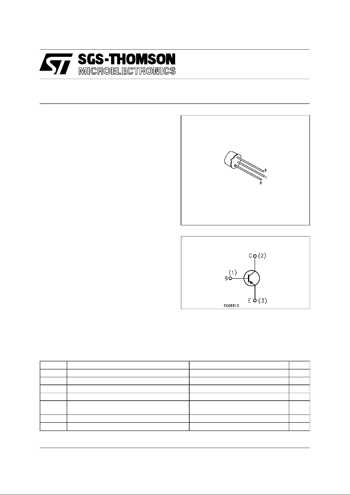
BFW43
HIGH VOLTAGE AMPLIFIER
TO-18
INTERNAL SCHEMATIC DIAGRAM
ABSOLUTE MAXIMUM RATINGS
Symb o l Parameter Val u e Uni t
V
V
V
P
T
Collector-Base V oltage (IE= 0) -150 V
CBO
Collector-Emitter V oltage (IB= 0) -150 V
CEO
Emitter-Base Voltage (IC=0) -6 V
EBO
Collect or Current -0. 1 A
I
C
Total Dissipati on at T
tot
Stora ge Temperat u re -55 to 200
stg
Max. Operating Juncti on Temperat ure 200
T
j
at T
amb
case
≤ 25oC
≤ 25oC
0.4
1.4
W
W
o
C
o
C
November 1997
1/5
Page 2

BFW43
THERMAL DATA
R
thj-case
R
thj- amb
Ther mal Resistance Junc t io n- Case Max
Thermal Resistance Junction-Ambient Max
125
438
o
C/W
o
C/W
ELECTRICAL CHARACTERISTICS (T
=25oC unlessotherwise specified)
case
Symbol Parameter Test Condition s Min. Typ. Max. Unit
I
V
(BR) CBO
CBO
Collector Cut-of f
Current (I
E
=0)
∗ Collect or- Base
=-100V
V
CE
V
=-100V T
CE
I
=-10µA-150V
C
amb
=125oC
-0.2
-0.03
-10
-10
Break dow n Volt age
=0)
(I
E
V
∗ Collect or- Emitt er
(BR) CEO
I
=-2mA -150 V
C
Break dow n Volt age
=0)
(I
B
V
(BR)EBO
∗ Em itt er-Base
I
=-10µA-6V
E
Break dow n Volt age
=0)
(I
C
V
∗ Co llector-E mitter
CE(sat)
IC=-10mA IB= - 1 mA -0. 1 -0.5 V
Saturation Voltage
V
BE(sat )
∗ Base-Emitt er
IC=-10mA IB= - 1 mA -0. 74 -0.9 V
Saturation Voltage
∗ DC Current Gain IC=-1mA VCE=-10V
h
FE
f
C
EBO
Tr ansition Frequenc y VCE=-10V f=20MHz
T
Emitt er Base
I
=-10mA VCE=-10V
C
=-10µAVCE= -10 V
I
C
T
=-55oC
amb
=-1mA
I
C
=-10mA 60
I
C
IE=0 VEB= - 0. 5 V f = 1MHz 20 25 pF
40
40
85
100
30
50 MHz
Capacit a nc e
C
CBO
Collector Base
IE=0 VCB=-5V f=1MHz 5 7 pF
Capacit a nc e
∗
Pulsed: Pulse duration = 300 µs, duty cycle≤ 1%
nA
µA
MHz
DCCurrent Gain. Collector-emitter SaturationVoltage.
2/5
Page 3

Base-emitterSaturationVoltage. TransitionFrequency.
BFW43
3/5
Page 4

BFW43
TO-18 MECHANICAL DATA
DIM.
MIN. TYP. MAX. MIN. TYP. MAX.
A 12.7 0.500
B 0.49 0.019
D 5.3 0.208
E 4.9 0.193
F 5.8 0.228
G 2.54 0.100
H 1.2 0.047
I 1.16 0.045
L45
o
mm inch
o
45
I
H
4/5
G
F
E
L
DA
B
C
0016043
Page 5

BFW43
Information furnishedis believed to be accurate and reliable. However,SGS-THOMSON Microelectronics assumes no responsability for the
consequencesof use ofsuch informationnorforanyinfringement of patents or other rights of third parties which may resultsfrom its use. No
licenseisgrantedby implicationor otherwise underany patent or patentrights ofSGS-THOMSON Microelectronics. Specificationsmentioned
in this publicationare subject tochange withoutnotice.This publication supersedes andreplaces all information previouslysupplied.
SGS-THOMSONMicroelectronics productsare notauthorizedforuseascriticalcomponents in lifesupportdevicesor systems withoutexpress
writtenapproval of SGS-THOMSON Microelectonics.
1997 SGS-THOMSONMicroelectronics- Printedin Italy - AllRights Reserved
Australia- Brazil - Canada - China - France- Germany- Italy - Japan - Korea - Malaysia - Malta- Morocco- The Netherlands -
Singapore- Spain- Sweden- Switzerland - Taiwan - Thailand - United Kingdom- U.S.A
SGS-THOMSONMicroelectronics GROUPOF COMPANIES
...
5/5
 Loading...