

Page 1

DISCRETE SEMICONDUCTORS
DATA SH EET
BFS505
NPN 9 GHz wideband transistor
Product specification
File under Discrete Semiconductors, SC14
September 1995
Page 2
Philips Semiconductors Product specification
NPN 9 GHz wideband transistor BFS505
FEATURES
• Low current consumption
• High power gain
• Low noise figure
• High transition frequency
• Gold metallization ensures
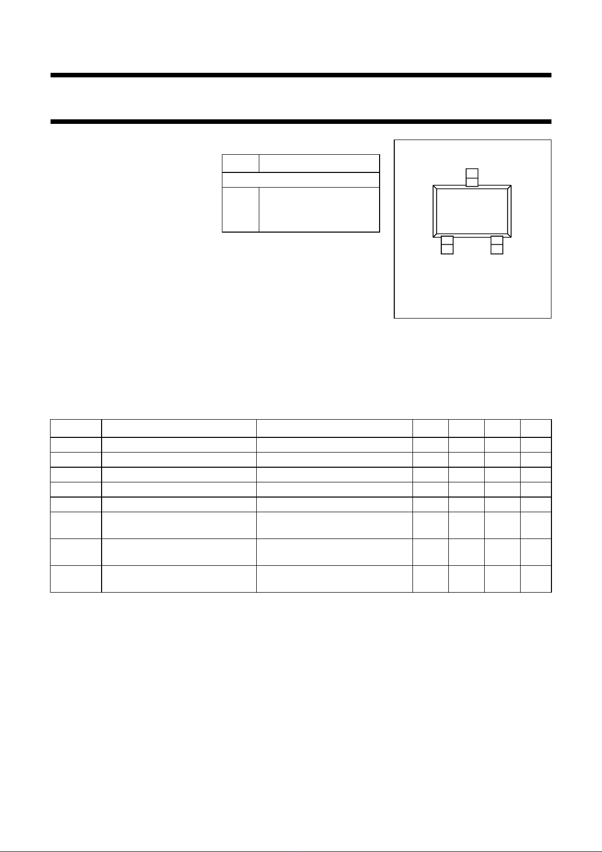
PINNING
PIN DESCRIPTION
Code: N0
1 base
2 emitter
3 collector
handbook, 2 columns
3
excellent reliability
• SOT323 envelope.
12
Top view
MBC870
DESCRIPTION
NPN transistor in a plastic SOT323
Fig.1 SOT323.
envelope.
It is intended for low power amplifiers,
oscillators and mixers particularly in
RF portable communication
equipment (cellular phones, cordless
phones, pagers) up to 2 GHz.
QUICK REFERENCE DATA
SYMBOL PARAMETER CONDITIONS MIN. TYP. MAX. UNIT
V
CBO
V
CES
I
C
P
tot
h
FE
f
T
G
UM
F noise figure I
collector-base voltage open emitter −−20 V
collector-emitter voltage RBE=0 −−15 V
DC collector current −−18 mA
total power dissipation up to Ts= 147 °C; note 1 −−150 mW
DC current gain IC= 5 mA; VCE= 6 V; Tj=25°C 60 120 250
transition frequency IC= 5 mA; VCE= 6 V; f = 1 GHz;
T
=25°C
amb
maximum unilateral power gain Ic= 5 mA; VCE= 6 V; f = 900 MHz;
T
=25°C
amb
= 1.25 mA; VCE=6 V;
c
f = 900 MHz; T
amb
=25°C
− 9 − GHz
− 17 − dB
− 1.2 1.7 dB
Note
is the temperature at the soldering point of the collector tab.
1. T
s
September 1995 2
Page 3

Philips Semiconductors Product specification
NPN 9 GHz wideband transistor BFS505
LIMITING VALUES
In accordance with the Absolute Maximum System (IEC 134).
SYMBOL PARAMETER CONDITIONS MIN. MAX. UNIT
V
CBO
V
CES
V
EBO
I
C
P
tot
T
stg
T
j
THERMAL RESISTANCE
SYMBOL PARAMETER CONDITIONS THERMAL RESISTANCE
R
th j-s
collector-base voltage open emitter − 20 V
collector-emitter voltage RBE=0 − 15 V
emitter-base voltage open collector − 2.5 V
DC collector current − 18 mA
total power dissipation up to Ts= 147 °C; note 1 − 150 mW
storage temperature −65 150 °C
junction temperature − 175 °C
thermal resistance from junction to
up to Ts= 147 °C; note 1 190 K/W
soldering point
Note
1. T
is the temperature at the soldering point of the collector tab.
s
September 1995 3
Page 4

Philips Semiconductors Product specification
NPN 9 GHz wideband transistor BFS505
CHARACTERISTICS
T
=25°C, unless otherwise specified.
j
SYMBOL PARAMETER CONDITIONS MIN. TYP. MAX. UNIT
I
CBO
h
FE
C
e
C
c
C
re
f
T
G
UM
2
S
21
F noise figure Γ
P
L1
ITO third order intercept point note 2 − 10 − dBm
collector cut-off current IE= 0; VCB=6 V −−50 nA
DC current gain IC= 5 mA; VCE= 6 V 60 120 250
emitter capacitance IC=ic= 0; VEB= 0.5 V; f = 1 MHz − 0.4 − pF
collector capacitance IE=ie= 0; VCB= 6 V; f = 1 MHz − 0.4 − pF
feedback capacitance IC= 0; VCB= 0.5 V; f = 1 MHz − 0.3 − pF
transition frequency IC= 5 mA; VCE= 6 V; f = 1 GHz;
T
=25°C
amb
maximum unilateral power gain
(note 1)
IC= 5 mA; VCE= 6 V; f = 900 MHz;
T
=25°C
amb
I
= 5 mA; VCE= 6 V; f = 2 GHz;
C
T
=25°C
amb
insertion power gain IC= 5 mA; VCE= 6 V; f = 900 MHz;
T
=25°C
amb
output power at 1 dB gain
compression
= Γ
s
f = 900 MHz; T
= Γ
Γ
s
f = 900 MHz; T
Γ
= Γ
s
f = 2 GHz; T
Ic= 5 mA; VCE= 6 V; RL=50Ω;
f = 900 MHz; T
= 1.25 mA; VCE=6 V;
opt;IC
=25°C
amb
= 5 mA; VCE=6 V;
opt;IC
=25°C
amb
= 1.25 mA; VCE=6 V;
opt;IC
=25°C
amb
=25°C
amb
− 9 − GHz
− 17 − dB
− 10 − dB
13 14 − dB
− 1.2 1.7 dB
− 1.6 2.1 dB
− 1.9 − dB
− 4 − dBm
Notes
1. G
2. I
is the maximum unilateral power gain, assuming S12is zero and
UM
G
UM
= 5 mA; VCE= 6 V; RL=50Ω; f = 900 MHz; T
C
--------------------------------------------------------------
10 log
1S
–
fp= 900 MHz; fq= 902 MHz; measured at f
2
S
21
2
1S
–
11
22
dB.=
2
=25°C;
amb
= 898 MHz and at f
(2p−q)
September 1995 4
(2p−q)
= 904 MHz.
Page 5

Philips Semiconductors Product specification
NPN 9 GHz wideband transistor BFS505
200
handbook, halfpage
P
tot
(mW)
150
100
50
0
0 50 100 200
150
Fig.2 Power derating curve.
MRC020 - 1
o
Ts(
C)
200
handbook, halfpage
h
FE
150
100
50
0
−3
10
VCE= 6 V; Tj=25°C.
−2
10
−1
10
11010
MRC019
I
(mA)
C
Fig.3 DC current gain as a function of collector
current.
2
0.5
handbook, halfpage
C
re
(pF)
0.4
0.3
0.2
0.1
0
0246810
IC= 0; f= 1 MHz.
V (V)
Fig.4 Feedback capacitance as a function of
collector-base voltage.
MRC011
CB
12
handbook, halfpage
f
T
(GHz)
10
8
6
4
2
0
−1
10
f = 1 GHz; T
amb
11010
=25°C.
= 8 V
V
CE
3 V
IC(mA)
Fig.5 Transition frequency as a function of
collector current.
MRC013
2
September 1995 5
Page 6

Philips Semiconductors Product specification
NPN 9 GHz wideband transistor BFS505
In Figs 6 to 9, GUM= maximum unilateral power gain;
MSG = maximum stable gain; G
gain.
= maximum available
max
25
handbook, halfpage
gain
(dB)
20
G
UM
15
10
5
0
02468
VCE= 6 V; f = 900 MHz; T
MSG
amb
=25°C.
Fig.6 Gain as a function of collector current.
MRC016
IC(mA)
20
handbook, halfpage
gain
(dB)
15
10
5
0
02468
VCE= 6 V; f = 2 GHz; T
amb
=25°C.
Fig.7 Gain as a function of collector current.
MSG
G
G
max
MRC017
UM
IC(mA)
50
handbook, halfpage
gain
(dB)
40
30
20
10
0
−2
10
IC= 1.25 mA; VCE= 6 V; T
G
UM
MSG
−1
10
=25°C.
amb
110
MRC015
G
max
f (GHz)
Fig.8 Gain as a function of frequency.
September 1995 6
50
handbook, halfpage
gain
(dB)
40
30
20
10
0
−2
10
IC= 5 mA; VCE= 6 V; T
Fig.9 Gain as a function of frequency.
MSG
10
amb
G
UM
−1
=25°C.
MRC014
G
max
110
f (GHz)
Page 7

Philips Semiconductors Product specification
NPN 9 GHz wideband transistor BFS505
handbook, halfpage
4
F
(dB)
3
2
1
0
10
VCE= 6 V; T
−1
f = 2 GHz
amb
900 MHz
500 MHz
=25°C.
110
I
(mA)
C
Fig.10 Minimum noise figure as a function of
collector current.
MRC018
handbook, halfpage
4
F
(dB)
3
2
1
0
−1
10
VCE= 6 V; T
amb
=25°C.
I = 5 mA
C
1.25 mA
110
f (GHz)
Fig.11 Minimum noise figure as a function of
frequency.
MRC012
September 1995 7
Page 8

Philips Semiconductors Product specification
NPN 9 GHz wideband transistor BFS505
handbook, full pagewidth
IC= 1.25 mA; VCE= 6 V;
f = 900 MHz; Z
o
=50Ω.
stability
circle
180°
0
−135°
135°
0.2
0.2
pot. unst.
region
0.5
0.2
0.5
90°
1
2
F
= 1. 2 dB
min
Γ
0.5 1 5
1
−90°
2
F = 1.5 dB
F = 2 dB
F = 3 dB
OPT
2
Fig.12 Noise circle.
45°
−45°
5
5
MRC073
1.0
0.8
0.6
0.4
0.2
0°
0
1.0
handbook, full pagewidth
IC= 1.25 mA; VCE= 6 V;
f = 2 GHz; Z
=50Ω.
o
180°
90°
1
135°
0
−135°
0.5
0.2
0.2 0.5 1 5
0.2
0.5
F = 4 dB
1
−90°
Fig.13 Noise circle.
F = 3 dB
F = 2.5 dB
F
= 1.9 dB
min
Γ
OPT
2
1.0
45°
2
5
5
2
−45°
MRC074
0.8
0.6
0.4
0.2
0°
0
1.0
September 1995 8
Page 9

Philips Semiconductors Product specification
NPN 9 GHz wideband transistor BFS505
handbook, full pagewidth
IC= 5 mA; VCE= 6 V;
=50Ω.
Z
o
90°
1
180°
135°
0
−135°
0.5
0.2
0.2 0.5 1 2 5
3 GHz
0.2
0.5
1
−90°
2
2
45°
40 MHz
−45°
Fig.14 Common emitter input reflection coefficient (S11).
5
5
MRC056
1.0
0.8
0.6
0.4
0.2
0°
0
1.0
handbook, full pagewidth
IC= 5 mA; VCE= 6 V.
90°
135°
180°
15 12 9 6 3
40 MHz
−135°
3 GHz
−90°
45°
0°
−45°
MRC057
Fig.15 Common emitter forward transmission coefficient (S21).
September 1995 9
Page 10

Philips Semiconductors Product specification
NPN 9 GHz wideband transistor BFS505
handbook, full pagewidth
IC= 5 mA; VCE= 6 V.
90°
135°
180°
0.5 0.4 0.3 0.2 0.1
−135°
3 GHz
40 MHz
−90°
45°
0°
−45°
MRC058
Fig.16 Common emitter reverse transmission coefficient (S12).
handbook, full pagewidth
IC= 5 mA; VCE= 6 V;
=50Ω.
Z
o
90°
1
180°
135°
0
−135°
0.5
0.2
0.2 0.5 1 2 5
0.2
0.5
1
−90°
3 GHz
45°
2
5
40 MHz
5
2
−45°
MRC059
Fig.17 Common emitter output reflection coefficient (S22).
1.0
0.8
0.6
0.4
0.2
0°
0
1.0
September 1995 10
Page 11

Philips Semiconductors Product specification
NPN 9 GHz wideband transistor BFS505
PACKAGE OUTLINE
Plastic surface mounted package; 3 leads SOT323
D
y
3
A
12
e
b
1
p
e
w M
B
E
H
E
A
1
detail X
AB
Q
L
p
X
v M
A
c
0 1 2 mm
scale
DIMENSIONS (mm are the original dimensions)
A
max
0.1
1
b
cD
p
0.4
0.25
0.10
2.2
1.8
0.3
IEC JEDEC EIAJ
E
1.35
1.15
REFERENCES
1.3
e
e
1
0.65
UNIT
A
1.1
mm
0.8
OUTLINE
VERSION
SOT323 SC-70
September 1995 11
H
E
2.2
2.0
L
p
0.45
0.15
Qwv
0.23
0.13
0.20.2
EUROPEAN
PROJECTION
ISSUE DATE
97-02-28
Page 12

Philips Semiconductors Product specification
NPN 9 GHz wideband transistor BFS505
DEFINITIONS
Data Sheet Status
Objective specification This data sheet contains target or goal specifications for product development.
Preliminary specification This data sheet contains preliminary data; supplementary data may be published later.
Product specification This data sheet contains final product specifications.
Limiting values
Limiting values given are in accordance with the Absolute Maximum Rating System (IEC 134). Stress above one or
more of the limiting values may cause permanent damage to the device. These are stress ratings only and operation
of the device at these or at any other conditions above those given in the Characteristics sections of the specification
is not implied. Exposure to limiting values for extended periods may affect device reliability.
Application information
Where application information is given, it is advisory and does not form part of the specification.
LIFE SUPPORT APPLICATIONS
These products are not designed for use in life support appliances, devices, or systems where malfunction of these
products can reasonably be expected to result in personal injury. Philips customers using or selling these products for
use in such applications do so at their own risk and agree to fully indemnify Philips for any damages resulting from such
improper use or sale.
September 1995 12
 Loading...