

Page 1

DISCRETE SEMICONDUCTORS
DATA SH EET
BFS17A
NPN 3 GHz wideband transistor
Product specification
File under Discrete Semiconductors, SC14
September1995
Page 2
Philips Semiconductors Product specification
NPN 3 GHz wideband transistor BFS17A
DESCRIPTION
NPN transistor in a plastic SOT23 package.
APPLICATIONS
• It is intended for RF applications such as oscillators
in TV tuners.
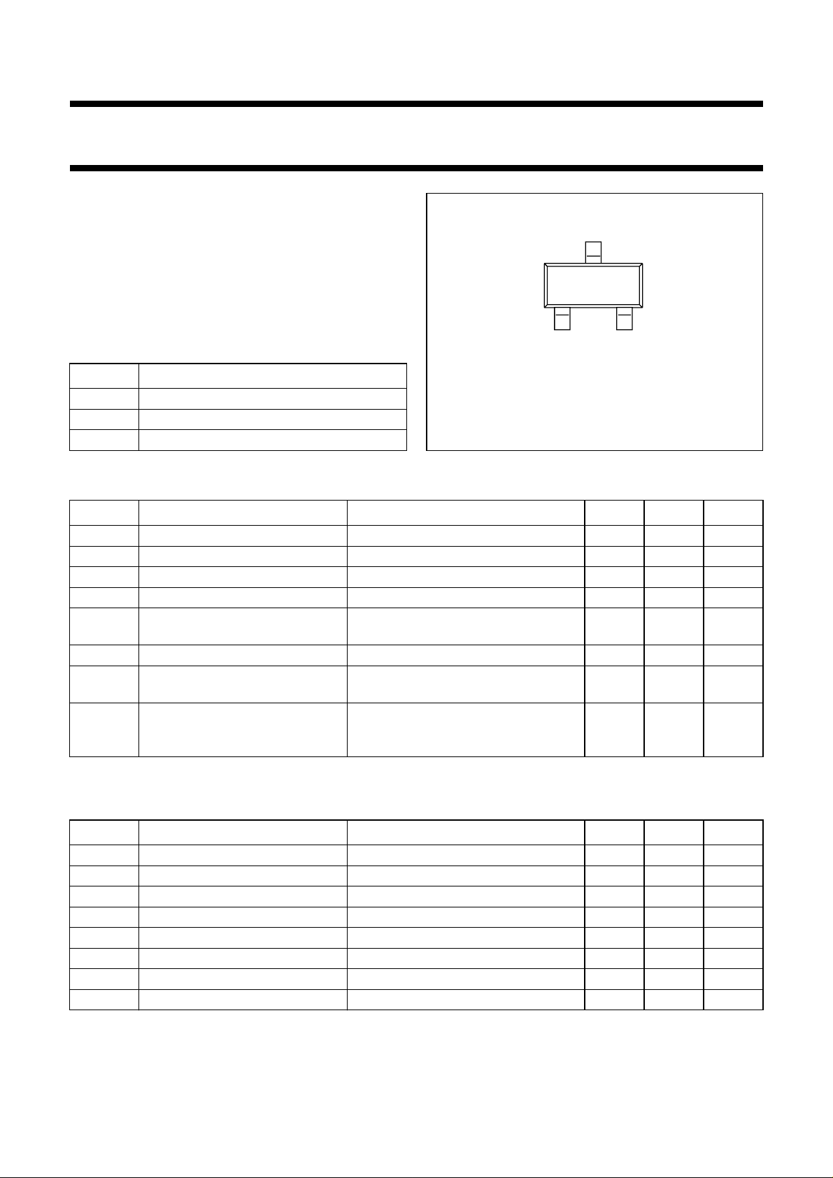
PINNING
PIN DESCRIPTION
1 base
2 emitter
3 collector
QUICK REFERENCE DATA
handbook, halfpage
12
Top view
Marking code: E2p.
Fig.1 SOT23.
3
MSB003
SYMBOL PARAMETER CONDITIONS TYP. MAX. UNIT
V
CBO
V
CEO
I
C
P
tot
f
T
G
UM
F noise figure I
V
O
collector-base voltage open emitter − 25 V
collector-emitter voltage open base − 15 V
DC collector current − 25 mA
total power dissipation up to Ts=70°C; note 1 − 300 mW
transition frequency IC= 25 mA; VCE= 5 V; f = 500 MHz;
T
=25°C
amb
2.8 − GHz
maximum unilateral power gain IC= 14 mA; VCE= 10 V; f = 800 MHz 13.5 − dB
= 2 mA; VCE= 5 V; f = 800 MHz;
C
T
=25°C
amb
output voltage dim= −60 dB; IC= 14 mA; VCE=10V;
RL=75Ω; T
f
= 793.25 MHz
(p+q−r)
amb
=25°C;
2.5 − dB
150 − mV
LIMITING VALUES
In accordance with the Absolute Maximum Rating System (IEC 134).
SYMBOL PARAMETER CONDITIONS MIN. MAX. UNIT
V
V
V
I
I
P
T
T
CBO
CEO
EBO
C
CM
tot
stg
j
collector-base voltage open emitter − 25 V
collector-emitter voltage open base − 15 V
emitter-base voltage open collector − 2.5 V
DC collector current − 25 mA
peak collector current − 50 mA
total power dissipation up to Ts=70°C; note 1 − 300 mW
storage temperature −65 +150 °C
junction temperature − 150 °C
Note to the Quick reference data and the Limiting values
is the temperature at the soldering point of the collector pin.
1. T
s
September1995 2
Page 3

Philips Semiconductors Product specification
NPN 3 GHz wideband transistor BFS17A
THERMAL CHARACTERISTICS
SYMBOL PARAMETER CONDITIONS VALUE UNIT
R
th j-s
Note
1. T
s
CHARACTERISTICS
=25°C unless otherwise specified.
T
j
SYMBOL PARAMETER CONDITIONS MIN. TYP. MAX. UNIT
I
CBO
h
FE
f
T
C
c
C
e
C
re
G
UM
F noise figure I
V
O
thermal resistance from junction to soldering point up to Ts=70°C; note 1 260 K/W
is the temperature at the soldering point of the collector pin.
collector cut-off current IE= 0; VCB=10V −−50 nA
DC current gain IC= 2 mA; VCE=1V; T
I
= 25 mA; VCE=1V; T
C
transition frequency IC= 25 mA; VCE= 5 V; f = 500 MHz;
T
=25°C
amb
collector capacitance IE= 0; VCB= 10 V; f = 1 MHz;
T
=25°C
amb
=25°C25 90 −
amb
=25°C25 90 −
amb
− 2.8 − GHz
− 0.7 − pF
emitter capacitance IC= 0; VEB= 0.5 V; f = 1 MHz − 1.25 − pF
feedback capacitance IC= 0; VCE=5V; f=1MHz − 0.6 − pF
maximum unilateral power gain
IC= 14 mA; VCE= 10 V; f = 800 MHz − 13.5 − dB
note 1
= 2 mA; VCE=5V; ZS=60Ω;
C
f = 800 MHz; T
amb
=25°C
− 2.5 − dB
output voltage note 2 − 150 − mV
Notes
1. G
is the maximum unilateral power gain, assuming S12 is zero and dB.
UM
2. dim= −60 dB (DIN 45004B); IC= 14 mA; VCE= 10 V; RL=75Ω; T
Vp=VO; fp= 795.25 MHz;
Vq=VO−6 dB; fq= 803.25 MHz;
Vr=VO−6 dB; fr= 805.25 MHz;
measured at f
= 793.25 MHz.
(p+q−r)
September1995 3
amb
G
=
UM
=25°C;
10 log
--------------------------------------------------------------
1S
–
11
2
S
21
2
1S
2
–
22
Page 4

Philips Semiconductors Product specification
NPN 3 GHz wideband transistor BFS17A
handbook, full pagewidth
L1=L3=5µH Ferroxcube choke.
L2 = 3 turns 0.4 mm copper wire; winding pitch 1 mm; internal diameter 3 mm.
V
BB
75 Ω
input
1.5 nF
1 nF
10 kΩ
L1
L2
270 Ω
3.3 pF
Fig.2 Intermodulation distortion and second order intermodulation distortion test circuit.
1 nF
1.5 nF
L3
DUT
18 Ω
1 nF
0.68 pF
MBB251
V
CC
75 Ω
output
100
handbook, halfpage
h
FE
50
0
0
VCE= 1 V; T
amb
10 30
=25°C.
20
MEA395
IC (mA)
Fig.3 DC current gain as a function of
collector current.
September1995 4
handbook, halfpage
1
C
c
(pF)
0.5
0
0
IE= 0; f = 1 MHz; T
4 8 12 16
=25°C.
amb
VCB (V)
Fig.4 Collector capacitance as a function of
collector-base voltage.
MEA903
Page 5

Philips Semiconductors Product specification
NPN 3 GHz wideband transistor BFS17A
handbook, halfpage
4
f
T
(GHz)
3
2
1
0
0
VCE= 5 V; f = 500 MHz; T
20 40
=25°C.
amb
IC (mA)
Fig.5 Transition frequency as a function of
collector current.
MEA904
handbook, halfpage
5
F
(dB)
4
3
2
1
0
0
VCE= 5 V; Zs=60Ω; f = 800 MHz; T
10 20
amb
IC (mA)
=25°C.
Fig.6 Minimum noise figure as a function of
collector current.
MEA902
September1995 5
Page 6

Philips Semiconductors Product specification
NPN 3 GHz wideband transistor BFS17A
PACKAGE OUTLINE
3.0
handbook, full pagewidth
0.55
0.45
0.150
0.090
2.8
1.9
0.95
21
B
A
M
A
0.2
30
max
0.1
max
max
o
2.5
1.4
max
M0.1 AB
1.2
MBC846
o
10
3
0.48
0.38
TOP VIEW
Dimensions in mm.
10
max
o
1.1
max
Fig.7 SOT23.
DEFINITIONS
Data sheet status
Objective specification This data sheet contains target or goal specifications for product development.
Preliminary specification This data sheet contains preliminary data; supplementary data may be published later.
Product specification This data sheet contains final product specifications.
Limiting values
Limiting values given are in accordance with the Absolute Maximum Rating System (IEC 134). Stress above one or
more of the limiting values may cause permanent damage to the device. These are stress ratings only and operation
of the device at these or at any other conditions above those given in the Characteristics sections of the specification
is not implied. Exposure to limiting values for extended periods may affect device reliability.
Application information
Where application information is given, it is advisory and does not form part of the specification.
LIFE SUPPORT APPLICATIONS
These products are not designed for use in life support appliances, devices, or systems where malfunction of these
products can reasonably be expected to result in personal injury. Philips customers using or selling these products for
use in such applications do so at their own risk and agree to fully indemnify Philips for any damages resulting from such
improper use or sale.
September1995 6
 Loading...