

Page 1

DISCRETE SEMICONDUCTORS
DATA SH EET
BFR94A
NPN 3.5 GHz wideband transistor
Product specification
File under Discrete Semiconductors, SC14
September 1995
Page 2
Philips Semiconductors Product specification
NPN 3.5 GHz wideband transistor BFR94A
DESCRIPTION
NPN resistance-stabilized transistor
in a SOT122E capstan envelope.
It features extremely low cross
modulation, intermodulation and
second order intermodulation
distortion. Due to its high transition
frequency, it has a high power gain, in
conjunction with good wideband
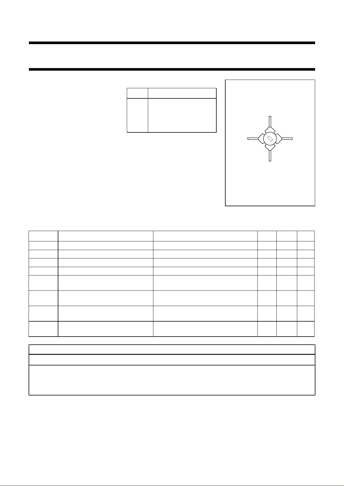
PINNING
PIN DESCRIPTION
1 collector
2 emitter
3 base
4 emitter
fpage
4
C
1
3
properties, and low noise up to high
frequencies.
2
MBB904
It is primarily intended for CATV and
MATV applications.
The BFR94A is a replacement for the
BFR94. The SOT122E footprint is
similar to that of the SOT48, used for
Fig.1 SOT122E.
the BFR94.
QUICK REFERENCE DATA
SYMBOL PARAMETER CONDITIONS TYP. MAX. UNIT
V
V
I
P
f
CBO
CEO
C
tot
T
collector-base voltage open emitter − 30 V
collector-emitter voltage open base − 25 V
DC collector current − 150 mA
total power dissipation up to Tc= 145 °C; f > 1 MHz − 3.5 W
transition frequency Ic= 90 mA; VCE= 20 V; f = 500 MHz;
3.5 − GHz
Tj=25°C
F noise figure I
d
im
d
2
intermodulation distortion Ic= 90 mA; VCE= 20 V;
second order intermodulation
distortion
= 90 mA; VCE= 20 V; f = 200 MHz;
c
=25°C
T
amb
Vo= 60 dBmV; f
= 194.25 MHz
(p+q−r)
Ic= 90 mA; VCE= 20 V;
Vo= 48 dBmV; fp+ fq= 210 MHz
810dB
−63 − dB
−−56 dB
WARNING
Product and environmental safety - toxic materials
This product contains beryllium oxide. The product is entirely safe provided that the BeO disc is not damaged. All
persons who handle, use or dispose of this product should be aware of its nature and of the necessary safety
precautions. After use, dispose of as chemical or special waste according to the regulations applying at the location of
the user. It must never be thrown out with the general or domestic waste.
September 1995 2
Page 3

Philips Semiconductors Product specification
NPN 3.5 GHz wideband transistor BFR94A
LIMITING VALUES
In accordance with the Absolute Maximum System (IEC 134).
SYMBOL PARAMETER CONDITIONS MIN. MAX. UNIT
V
CBO
V
CEO
V
CER
V
EBO
I
C
I
CM
P
tot
T
stg
T
j
THERMAL RESISTANCE
collector-base voltage open emitter − 30 V
collector-emitter voltage open base − 25 V
collector-emitter voltage RBE= 100 Ω−35 V
emitter-base voltage open collector − 3V
DC collector current − 150 mA
peak collector current f > 1 MHz − 300 mA
total power dissipation up to Tc= 145 °C; f > 1 MHz − 3.5 W
storage temperature −65 200 °C
junction temperature − 200 °C
SYMBOL PARAMETER THERMAL RESISTANCE
R
th j-c
thermal resistance from junction to case 15 K/W
September 1995 3
Page 4

Philips Semiconductors Product specification
NPN 3.5 GHz wideband transistor BFR94A
CHARACTERISTICS
T
=25°C unless otherwise specified.
j
SYMBOL PARAMETER CONDITIONS MIN. TYP. MAX. UNIT
I
CBO
h
FE
f
T
C
c
C
e
C
re
C
cs
G
UM
F noise figure I
d
im
d
2
V
o
collector cut-off current IE= 0; VCB= 20 V −−50 µA
DC current gain IC= 50 mA; VCE= 20 V 30 −−
I
= 150 mA; VCE= 20 V 30 −−
C
transition frequency IC= 90 mA; VCE= 20 V; f = 500 MHz − 3.5 − GHz
I
= 150 mA; VCE= 20 V;
C
− 3.5 − GHz
f = 500 MHz
collector capacitance IE=ie= 0; VCB= 20 V; f = 1 MHz − 3.5 − pF
emitter capacitance IC=ic= 0; VEB= 0.5 V; f = 1 MHz − 12 − pF
feedback capacitance IC= 10 mA; VCE= 20 V; f = 1 MHz − 1.3 − pF
collector-stud capacitance f = 1 MHz − 2 − pF
maximum unilateral power gain
(note 1)
IC= 90 mA; VCE= 20 V;
f = 500 MHz; T
= 90 mA; VCE= 20 V;
C
f = 200 MHz; T
I
= 90 mA; VCE= 20 V;
C
f = 500 MHz; T
amb
amb
amb
=25°C
=25°C
=25°C
− 13.5 − dB
− 810dB
− 5 − dB
intermodulation distortion note 2 −−63 − dB
second order intermodulation
note 3 −−−56 dB
distortion
output voltage see Fig.2 and note 4 − 700 − mV
Notes
1. G
2. I
is the maximum unilateral power gain, assuming S12is zero and
UM
G
UM
= 90 mA; VCE= 20 V; RL=75Ω;
C
--------------------------------------------------------------
10 log
1S
–
2
S
21
2
–
1S
11
22
dB.=
2
Vp=Vo= 60 dBmV at fp= 196.25 MHz;
Vq=Vo−6 dB at fq= 203.25 MHz;
Vr=Vo−6 dB at fr= 205.25 MHz;
measured at f
) = 194.25 MHz.
(p+q−r
3. IC= 90 mA; VCE= 20 V;
fp= 66 MHz; fq= 144 MHz; fp+ fq= 210 MHz; Vo= 48 dBmV.
4. dim= −60 dB (DIN 45004B); Ic= 90 mA; VCE= 20 V; RL=75Ω; T
Vp=Vo at dim= −60 dB; fp= 495.25 MHz;
Vq=Vo−6 dB; fq= 503.25 MHz;
Vr=Vo−6 dB; fr= 505.25 MHz;
measured at f
= 493.25 MHz.
(p+q−r)
amb
=25°C;
September 1995 4
Page 5

Philips Semiconductors Product specification
NPN 3.5 GHz wideband transistor BFR94A
handbook, halfpage
75 Ω
L1=L2=5µH Ferroxcube choke, catalogue
number 3122 108 20153.
2.2 nF
V
BB
1.5 kΩ
L1
10 nF
240 Ω
1 nF
19 Ω
2.2 nF
L2
10 nF
DUT
MEA497
Fig.2 Intermodulation distortion MATV test circuit.
V
CC
75 Ω
handbook, halfpage
4
f
T
(GHz)
3
2
1
0
VCE= 20 V; f= 500 MHz; Tj=25°C.
1010
2
I (mA)
C
Fig.3 Transition frequency as a function of
collector current.
MEA496
3
10
30
handbook, halfpage
d
im
(dB)
40
50
60
70
80
0 150
Measured in CATV test circuit.
VCE= 20 V; Vo= 60 dBmV;
= 194. 25 MHz.
f
(p+q−r)
50 100
MEA495
I (mA)
C
Fig.4 Intermodulation distortion as a function of
collector current.
30
handbook, halfpage
d
2
(dB)
40
50
60
70
80
0 150
Measured in CATV test circuit.
VCE= 20 V; Vo= 48 dBmV; f = 210 MHz.
50 100
MEA494
I (mA)
C
Fig.5 Second order intermodulation distortion as
a function of collector current.
September 1995 5
Page 6

Philips Semiconductors Product specification
NPN 3.5 GHz wideband transistor BFR94A
handbook, full pagewidth
IC= 90 mA; VCE= 20 V; T
Zo=50Ω.
amb
1
0.5
0.2
+ j
0
– j
0.2
0.5
=25°C.
1000 MHz
800
10.2 10520.5
500
200
100
1
Fig.6 Common emitter input reflection coefficient (S11).
2
5
10
∞
10
5
2
MEA498
handbook, full pagewidth
IC= 90 mA; VCE= 20 V; T
90°
60°
60°
amb
180°
=25°C.
150°
150°
120°
100 MHz
200
500
90°
800
1000
20
10
120°
Fig.7 Common emitter forward transmission coefficient (S21).
30°
+ ϕ
0°
− ϕ
30°
MEA900
September 1995 6
Page 7

Philips Semiconductors Product specification
NPN 3.5 GHz wideband transistor BFR94A
handbook, full pagewidth
IC= 90 mA; VCE= 20 V; T
90°
800
60°
1000 MHz
60°
amb
180°
=25°C.
150°
150°
120°
500
200
0.20.3
120°
0.1
100
90°
Fig.8 Common emitter reverse transmission coefficient (S12).
30°
+ ϕ
0°
− ϕ
30°
MEA901
handbook, full pagewidth
IC= 90 mA; VCE= 20 V; T
Zo=50Ω.
amb
1
0.5
0.2
+ j
0
– j
500
0.2
0.5
=25°C.
1000
10.2 10520.5
200
1
100 MHz
Fig.9 Common emitter output reflection coefficient (S22).
2
5
10
∞
10
5
2
MEA499
September 1995 7
Page 8

Philips Semiconductors Product specification
NPN 3.5 GHz wideband transistor BFR94A
PACKAGE OUTLINE
Studded ceramic package; 4 leads SOT122E
D
A
Q
N
1
N
2
N
N
3
L
H
1
D
1
D
2
H
b
2
b
4
C
ceramic
BeO
metal
A
X
c
w
A
M
1
M
M
1
detail X
W
α
3
b
1
2
0 5 10 mm
scale
DIMENSIONS (millimetre dimensions are derived from the original inch dimensions)
D
UNIT A
5.97
mm
4.80
OUTLINE
VERSION
SOT122E
1.05
0.73
b1b
10.75
10.43
cM
2
14.25
0.18
13.94
0.14
IEC JEDEC EIAJ
Db
7.50
7.23
D
1
6.46
7.19
6.25
6.93
REFERENCES
H
27.56
25.78
L
6.84
5.30
2
September 1995 8
3.18
2.92
M
1.63
1.42
N
1
N
1
11.82
11.04
N
N3Q
max.
1.02 0.381
2
8.89
3.68
7.36
2.92
EUROPEAN
PROJECTION
3.38
2.79
W
w
8-32
UNC
ISSUE DATE
97-04-18
α
1
90°
Page 9

Philips Semiconductors Product specification
NPN 3.5 GHz wideband transistor BFR94A
DEFINITIONS
Data Sheet Status
Objective specification This data sheet contains target or goal specifications for product development.
Preliminary specification This data sheet contains preliminary data; supplementary data may be published later.
Product specification This data sheet contains final product specifications.
Limiting values
Limiting values given are in accordance with the Absolute Maximum Rating System (IEC 134). Stress above one or
more of the limiting values may cause permanent damage to the device. These are stress ratings only and operation
of the device at these or at any other conditions above those given in the Characteristics sections of the specification
is not implied. Exposure to limiting values for extended periods may affect device reliability.
Application information
Where application information is given, it is advisory and does not form part of the specification.
LIFE SUPPORT APPLICATIONS
These products are not designed for use in life support appliances, devices, or systems where malfunction of these
products can reasonably be expected to result in personal injury. Philips customers using or selling these products for
use in such applications do so at their own risk and agree to fully indemnify Philips for any damages resulting from such
improper use or sale.
September 1995 9
 Loading...