

Page 1
NPN Silicon RF Transistor
BFR 93A
For low-noise, high-gain broadband amplifiers at
collector currents from 2 mA to 30 mA
1
ESD: Electrostatic discharge sensitive device, observe handling precaution!
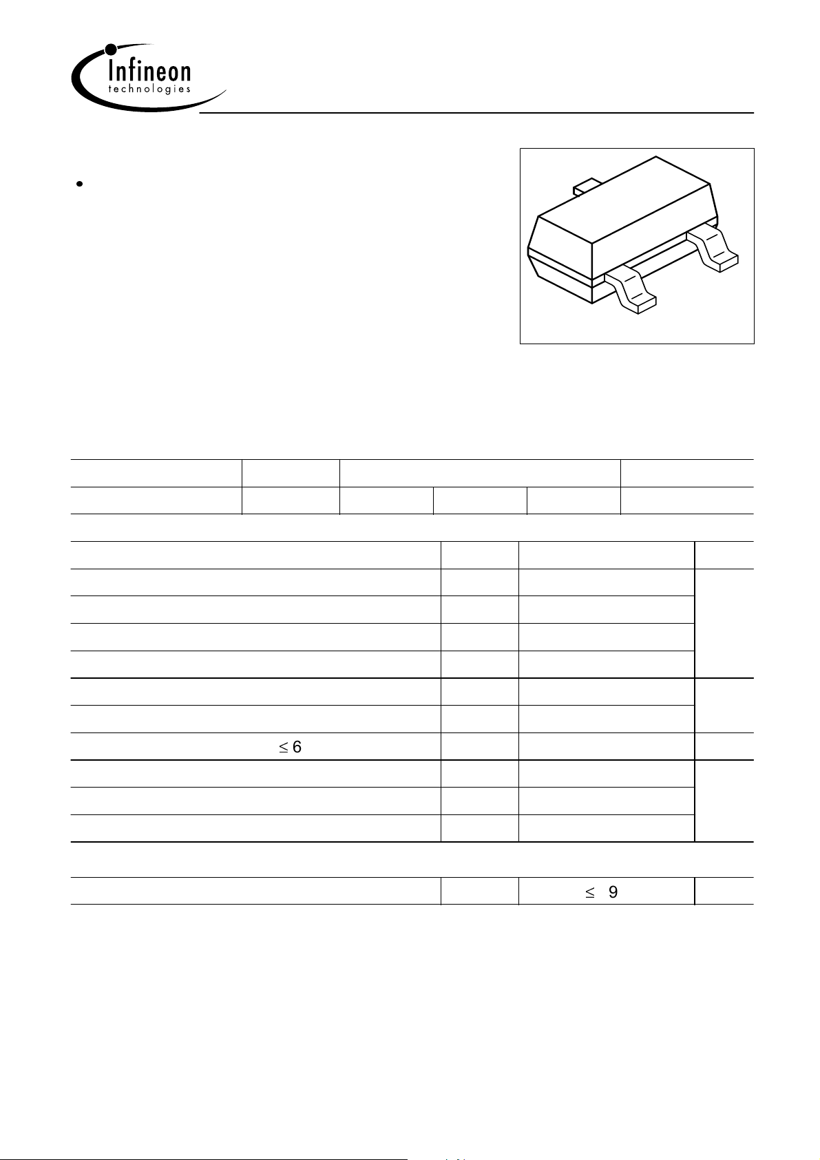
Type Marking Pin Configuration Package
BFR 93A R2s 1 = B 2 = E 3 = C SOT-23
Maximum Ratings
3
Parameter
Symbol UnitValue
2
VPS05161
Collector-emitter voltage 12V
Collector-emitter voltage V
Collector-base voltage 20V
Emitter-base voltage
Collector current I
Base current I
Total power dissipation, TS 63 °C
1)
Junction temperature T
Ambient temperature T
Storage temperature T
Thermal Resistance
Junction - soldering point
C
B
P
R
CEO
CES
CBO
EBO
tot
j
A
stg
thJS
20
2V
50 mA
6
300 mW
150 °C
-65 ... 150
-65 ... 150
290
V
K/W
1
T
is measured on the collector lead at the soldering point to the pcb
S
Oct-13-19991
Page 2

Electrical Characteristics at TA = 25°C, unless otherwise specified.
BFR 93A
Parameter
DC characteristics
Collector-emitter breakdown voltage
= 1 mA, IB = 0
I
C
Collector-emitter cutoff current
V
= 20 V, VBE = 0
CE
Collector-base cutoff current
V
= 10 V, IE = 0
CB
Emitter-base cutoff current
= 2 V, IC = 0
V
EB
DC current gain
= 30 mA, VCE = 8 V
I
C
Symbol Values Unit
min. typ. max.
V
(BR)CEO
I
CES
I
CBO
I
EBO
h
FE
12 - - V
- - 100 µA
- - 100 nA
- - 10 µA
50 100 200 -
Oct-13-19992
Page 3

Electrical Characteristics at TA = 25°C, unless otherwise specified.
BFR 93A
Parameter
AC characteristics (verified by random sampling)
Transition frequency
= 30 mA, VCE = 8 V, f = 500 MHz
I
C
Collector-base capacitance
= 10 V, f = 1 MHz
V
CB
Collector-emitter capacitance
= 10 V, f = 1 MHz
V
CE
Emitter-base capacitance
= 0.5 V, f = 1 MHz
V
EB
Noise figure
= 5 mA, VCE = 8 V, ZS = Z
I
C
Sopt
,
f = 900 MHz
f = 1.8 GHz
Symbol Values Unit
min. typ. max.
f
C
C
C
F
T
cb
ce
eb
4.5 6 - GHz
- 0.58 0.9 pF
- 0.23 -
- 1.7 -
-
-
2
3.3
dB
-
-
Power gain, maximum available 1)
= 30 mA, VCE = 8 V, ZS = Z
I
C
Sopt
, ZL = Z
f = 900 MHz
f = 1.8 GHz
Transducer gain
= 30 mA, VCE = 8 V, ZS = ZL = 50 ,
I
C
f = 900 MHz
f = 1.8 GHz
Lopt
,
G
|S
ma
21e
-
-
2
|
-
-
13.5
8.5
12
6.5
-
-
-
-
1
G
= |S21 / S12| (k-(k2-1)
ma
1/2
)
Oct-13-19993
Page 4

SPICE Parameters (Gummel-Poon Model, Berkley-SPICE 2G.6 Syntax) :
Transistor Chip Data
BFR 93A
IS = 8.6752 fA
VAF = 20.011 V
NE = 1.5466 -
VAR = 26.834 V
NC = 1.95 -
RBM = 3.4649
CJE = 3.1538 fF
TF = 33.388 ps
ITF = 2.5184 mA
VJC = 0.72744 V
TR = 1.1061 ns
MJS = 0-
XTI = 3 -
All parameters are ready to use, no scalling is necessary.
Extracted on behalf of SIEMENS Small Signal Semiconductors by:
Institut für Mobil-und Satellitentechnik (IMST)
1996 SIEMENS AG
BF = 137.63 -
IKF = 0.33395 A
BR = 59 -
IKR = 0.015129 A
RB = 7.2326
RE = 1.0075
VJE = 0.70393 V
XTF = 0.28319 -
PTF = 0 deg
MJC = 0.34565 -
CJS = 0fF
XTB = 0-
FC = 0.75935 -
NF = 0.93633 -
ISE = 2619.3 fA
NR = 0.88761 -
ISC = 0.70823 fA
IRB = 0.043806 mA
RC = 0.13193
MJE = 0.5071 -
VTF = 0.17765 V
CJC = 1039.5 fF
XCJC = 0.21422 -
VJS = 0.75 V
EG = 1.11 eV
TNOM 300 K
Package Equivalent Circuit:
LBI =
=
L
BO
L
=
EI
L
=
EO
=
L
CI
=
L
CO
C
=
BE
=
C
CB
=
C
CE
Valid up to 6GHz
For examples and ready to use parameters please contact your local Infineon Technologies distributor or sales
office to obtain a Infineon Technologies CD-ROM or see Internet: http://www.infineon.com/products/discrete/index.htm
0.85 nH
0.51 nH
0.69 nH
0.61 nH
0nH
0.49 nH
73 fF
84 fF
165 fF
Oct-13-19994
Page 5

BFR 93A
Total power dissipation P
* Package mounted on epoxy
400
mW
300
tot
250
P
200
150
100
50
0
0 20 40 60 80 100 120
T
A
= f (TA*, TS)
tot
T
S
°C
TA,T
150
S
Permissible Pulse Load R
3
10
K/W
2
10
thJS
R
1
10
0
10
-7
-6
-5
10
10
10
10
-4
10
thJS
0.5
0.2
0.1
0.05
0.02
0.01
0.005
D = 0
-3
= f (tp)
-2
10
s
tp
10
Permissible Pulse Load
P
totmax/PtotDC
2
10
totDC
-
/ P
totmax
P
1
10
0
0
10
10
-7
10
= f (tp)
-6
-5
10
10
D = 0
0.005
0.01
0.02
0.05
0.1
0.2
0.5
-4
-3
10
10
-2
s
10
0
tp
Oct-13-19995
Page 6

BFR 93A
Collector-base capacitance Ccb = f (VCB)
f = 1MHz
1.5
pF
1.2
1.1
1.0
cb
C
0.9
0.8
0.7
0.6
0.5
0.4
0.3
0.2
0.1
0.0
0 4 8 12 16
V
VCB
22
Transition frequency fT = f (IC)
VCE = Parameter
6.0
GHz
5.0
4.5
4.0
T
f
3.5
3.0
2.5
2.0
1.5
1.0
0.5
0.0
0 10 20 30 40
10V
mA
2V
1V
0.7V
60
IC
Power Gain Gma, Gms = f(IC)
f = 0.9GHz
= Parameter
V
CE
14
dB
G
10
8
6
4
0 10 20 30 40
10V
mA
5V
3V
2V
1V
0.7V
IC
60
Power Gain Gma, Gms = f(IC)
f = 1.8GHz
= Parameter
V
CE
9
dB
7
6
G
5
4
3
2
1
0 10 20 30 40
10V
mA
5V
3V
2V
1V
0.7V
60
IC
Oct-13-19996
Page 7

BFR 93A
Power Gain Gma, Gms = f(VCE):_____
|S21|2 = f(VCE):---------
f = Parameter
16
IC=30mA
dB
12
G
10
8
6
4
2
0 2 4 6 8
0.9GHz
0.9GHz
1.8GHz
1.8GHz
V
VCE
12
Intermodulation Intercept Point IP3=f(IC)
(3rd order, Output, ZS=ZL=50)
= Parameter, f = 900MHz
V
CE
32
dBm
28
26
3
24
IP
22
20
18
16
14
12
10
0 10 20 30 40
8V
1V
mA
5V
3V
2V
60
IC
Power Gain Gma, Gms = f(f)
V
= Parameter
CE
32
IC=30mA
dB
24
20
G
16
12
8
4
0
0.0 0.5 1.0 1.5 2.0 2.5
GHz
10V
1V
0.7V
3.5
Power Gain |S21|2= f(f)
VCE = Parameter
30
IC=30mA
dB
22
21
18
S
14
10
6
2
-2
0.0 0.5 1.0 1.5 2.0 2.5
GHz
10V
1V
0.7V
3.5
f
f
Oct-13-19997
 Loading...