

Page 1

DISCRETE SEMICONDUCTORS
DATA SH EET
BFR92AW
NPN 5 GHz wideband transistor
Product specification
Supersedes data of October 1992
File under discrete semiconductors, SC14
1995 Sep 18
Page 2
Philips Semiconductors Product specification
NPN 5 GHz wideband transistor BFR92AW
FEATURES
• High power gain
• Gold metallization ensures
excellent reliability
• SOT323 (S-mini) package.
APPLICATIONS
It is designed for use in RF amplifiers,
mixers and oscillators with signal
frequencies up to 1 GHz.
DESCRIPTION
Silicon NPN transistor encapsulated
in a plastic SOT323 (S-mini) package.
The BFR92AW uses the same crystal
as the SOT23 version, BFR92A.
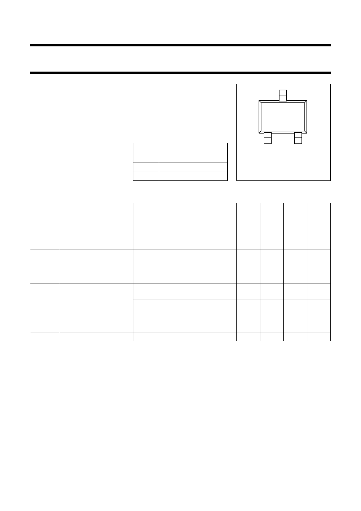
PINNING
PIN DESCRIPTION
1 base
2 emitter
3 collector
handbook, 2 columns
Top view
Marking code: P2.
Fig.1 SOT323
3
12
MBC870
QUICK REFERENCE DATA
SYMBOL PARAMETER CONDITIONS MIN. TYP. MAX. UNIT
V
CBO
V
CEO
I
C
P
tot
h
FE
C
re
f
T
G
UM
F noise figure I
T
j
collector-base voltage open emitter −−20 V
collector-emitter voltage open base −−15 V
collector current (DC) −−25 mA
total power dissipation up to Ts=93°C; note 1 −−300 mW
current gain IC= 15 mA; VCE=10V 40 90 −
feedback capacitance IC= 0; VCE= 10 V; f = 1 MHz;
T
=25°C
amb
− 0.35 − pF
transition frequency IC= 15 mA; VCE= 10 V; f = 500 MHz 3.5 5 − GHz
maximum unilateral power
gain
IC= 15 mA; VCE= 10 V; f = 1 GHz;
T
=25°C
amb
I
= 15 mA; VCE= 10 V; f = 2 GHz;
C
T
=25°C
amb
= 5 mA; VCE= 10 V; f = 1 GHz;
C
Γs= Γ
opt
− 14 − dB
− 8 − dB
− 2 − dB
junction temperature −−150 °C
Note
1. T
is the temperature at the soldering point of the collector pin.
s
1995 Sep 18 2
Page 3
Philips Semiconductors Product specification
NPN 5 GHz wideband transistor BFR92AW
LIMITING VALUES
In accordance with the Absolute Maximum System (IEC 134).
SYMBOL PARAMETER CONDITIONS MIN. MAX. UNIT
V
CBO
V
CEO
V
EBO
I
C
P
tot
T
stg
T
j
THERMAL CHARACTERISTICS
SYMBOL PARAMETER CONDITIONS VALUE UNIT
R
th j-s
collector-base voltage open emitter − 20 V
collector-emitter voltage open base − 15 V
emitter-base voltage open collector − 2V
collector current (DC) − 25 mA
total power dissipation up to Ts=93°C; see Fig.2; note 1 − 300 mW
storage temperature −65 +150 °C
junction temperature − 150 °C
thermal resistance from junction to
up to Ts=93°C; note 1 190 K/W
soldering point
Note to the Limiting values and Thermal characteristics
1. T
is the temperature at the soldering point of the collector pin.
s
150
MLB540
o
T ( C)
s
400
P
tot
(mW)
300
200
100
0
0 50 100 200
Fig.2 Power derating curve
1995 Sep 18 3
Page 4

Philips Semiconductors Product specification
NPN 5 GHz wideband transistor BFR92AW
CHARACTERISTICS
T
=25°C (unless otherwise specified).
j
SYMBOL PARAMETER CONDITIONS MIN. TYP. MAX. UNIT
I
CBO
h
FE
C
c
C
e
C
re
f
T
G
UM
F noise figure I
collector leakage current IE= 0; VCB=10V −−50 nA
DC current gain IC= 15 mA; VCE= 10 V 40 90 −
collector capacitance IE=ie= 0; VCB= 10 V; f = 1 MHz − 0.6 − pF
emitter capacitance IC=ic= 0; VEB= 0.5 V; f = 1 MHz − 0.9 − pF
feedback capacitance IC= 0; VCE= 10 V; f = 1 MHz − 0.35 − pF
transition frequency IC= 15 mA; VCE= 10 V; f = 500 MHz 3.5 5 − GHz
maximum unilateral power
gain; note 1
IC= 15 mA; VCE=10V;
f = 1 GHz; T
I
= 15 mA; VCE=10V;
C
f = 2 GHz; T
= 5 mA; VCE=10V;
C
f = 1 GHz; Γs= Γ
I
= 5 mA; VCE=10V;
C
f = 2 GHz; Γs= Γ
amb
amb
=25°C
=25°C
opt
opt
− 14 − dB
− 8 − dB
− 2 − dB
− 3 − dB
Note
1. G
is the maximum unilateral power gain, assuming s12 is zero and
UM
2
s
G
UM
10
-----------------------------------------------------------1s
–()1s
21
2
11
–()
dB.log=
2
22
1995 Sep 18 4
Page 5

Philips Semiconductors Product specification
NPN 5 GHz wideband transistor BFR92AW
I (mA)
C
MCD074
120
handbook, halfpage
h
FE
80
40
0
0102030
VCE=10V.
Fig.3 DC current gain as a function of collector
current; typical values.
1.0
C
re
(pF)
0.8
0.6
0.4
0.2
0
0
IC= 0; f= 1 MHz.
48
12 16
MGC883
V (V)
CB
Fig.4 Feedback capacitance as a function of
collector-base voltage; typical values.
20
handbook, halfpage
6
f
T
(GHz)
4
2
0
VCE= 5 V; f = 500 MHz; T
amb
101
=25°C.
I (mA)
C
Fig.5 Transition frequency as a function of
collector current; typical values.
MGC884
2
10
1995 Sep 18 5
Page 6

Philips Semiconductors Product specification
NPN 5 GHz wideband transistor BFR92AW
30
handbook, halfpage
gain
(dB)
20
10
0
0
VCE= 10 V; f = 500 MHz.
510
MSG
G
15 20
Fig.6 Gain as a function of collector current;
typical values.
MGC885
UM
I (mA)
C
30
handbook, halfpage
gain
(dB)
20
MSG
G
10
0
0
VCE= 10 V; f = 1 GHz.
510
15 20
Fig.7 Gain as a function of collector current;
typical values.
MGC886
UM
I (mA)
C
50
handbook, halfpage
gain
(dB)
VCE=10V;IC= 5 mA.
G
40
MSG
30
20
10
0
10
Fig.8 Gain as a function of frequency;
UM
2
10
typical values.
MGC887
G
max
3
10
f (MHz)
4
10
50
handbook, halfpage
gain
(dB)
VCE=10V;IC=15mA.
G
UM
40
MSG
30
20
10
0
10
2
10
3
10
G
f (MHz)
MGC888
max
4
10
Fig.9 Gain as a function of frequency;
typical values.
1995 Sep 18 6
Page 7

Philips Semiconductors Product specification
NPN 5 GHz wideband transistor BFR92AW
handbook, halfpage
6
F
(dB)
4
2
0
VCE=10V.
101
f = 2 GHz
1 GHz
500 MHz
I (mA)
C
Fig.10 Minimum noise figure as a function of
collector current; typical values.
MGC889
handbook, halfpage
2
10
6
F
(dB)
4
2
0
2
10
VCE=10V.
3
10
IC = 15 mA
10 mA
5 mA
f (MHz)
MGC890
10
4
Fig.11 Minimum noise figure as a function of
frequency; typical values.
handbook, full pagewidth
o
180
f = 500 MHz; VCE= 10 V; IC= 5 mA; Zo=50Ω.
Fig.12 Common emitter noise figure circles; typical values.
o
90
1
o
135
0
135
0.2
0.2
0.5
0.50.2
0.5
o
1
1
o
90
F = 4 dB
F = 3 dB
F = 2 dB
F = 1.6 dB
min
Γ
opt
2 5
o
45
2
5
5
2
o
45
MGC891
1.0
0.8
0.6
0.4
0.2
o
00
1.0
1995 Sep 18 7
Page 8

Philips Semiconductors Product specification
NPN 5 GHz wideband transistor BFR92AW
o
90
handbook, full pagewidth
180
1
135
o
0.5
o
45
2
(4)
(3)
0.2
(5)
(6)
o
0.2
0
0.5
(2)
5
(1)
21 5
(7)
1.0
0.8
0.6
0.4
0.2
o
00
(1) Γ
; F
= 2.1 dB.
opt
min
(2) F = 2.5 dB.
(3) F = 3 dB.
(4) F = 4 dB.
(5) Γms;G
= 15.7 dB.
max
(6) G = 15 dB.
(7) G = 14 dB.
(8) G = 13 dB.
f = 1 GHz; VCE= 10 V; IC= 5 mA; Zo=50Ω.
handbook, full pagewidth
0.2
135
(8)
0.5
o
2
1
o
90
5
o
45
MGC892
Fig.13 Common emitter noise figure circles; typical values.
o
90
1
180
o
135
0.5
(4)
(3)
(1)
(2)
21 5
0.2
o
0.2
0
0.5
(5)
o
45
2
5
1.0
1.0
0.8
0.6
0.4
0.2
o
00
(1) Γ
; F
opt
min
(2) F = 3.5 dB.
(3) F = 4 dB.
(4) F = 5 dB.
(5) Γms;G
max
0.2
= 3 dB.
135
= 9.1 dB.
(6)
(7)
(8)
0.5
o
(6) G = 8 dB.
(7) G = 7 dB.
(8) G = 6 dB.
f = 2 GHz; VCE= 10 V; IC= 5 mA; Zo=50Ω.
Fig.14 Common emitter noise figure circles; typical values.
1995 Sep 18 8
5
2
1
o
90
o
45
MGC893
1.0
Page 9

Philips Semiconductors Product specification
NPN 5 GHz wideband transistor BFR92AW
o
90
handbook, full pagewidth
135
1
o
0.5
o
45
2
1.0
0.8
0.6
VCE= 10 V; IC= 15 mA; Zo=50Ω.
handbook, full pagewidth
0.4
0.2
o
00
180
0.2
5
3 GHz
o
0.2 1
0
0.5
2
5
40 MHz
0.2
135
0.5
o
2
1
o
90
5
o
45
MGC894
1.0
Fig.15 Common emitter input reflection coefficient (s11); typical values.
o
90
135
o
o
45
135
40 MHz
o
o
180
50 40 30 20 10
VCE= 10 V; IC=15mA.
Fig.16 Common emitter forward transmission coefficient (s21); typical values.
1995 Sep 18 9
90
3 GHz
o
o
0
o
45
MGC895
Page 10

Philips Semiconductors Product specification
NPN 5 GHz wideband transistor BFR92AW
o
handbook, full pagewidth
90
VCE= 10 V; IC=15mA.
o
135
o
180
0.25 0.20 0.15 0.10 0.05
o
135
90
40 MHz
o
o
45
o
0
o
45
MGC896
Fig.17 Common emitter reverse transmission coefficient (s12); typical values.
3 GHz
handbook, full pagewidth
VCE= 10 V; IC= 15 mA; Zo=50Ω.
Fig.18 Common emitter output reflection coefficient (s22); typical values.
180
o
90
1.0
0.8
135
1
o
0.5
o
45
2
0.6
0.2
5
0.4
0.2
o
0.2 0.5 2
0
1 5
o
00
40 MHz
0.2
135
0.5
o
1
90
3 GHz
2
o
5
o
45
MGC897
1.0
1995 Sep 18 10
Page 11

Philips Semiconductors Product specification
NPN 5 GHz wideband transistor BFR92AW
PACKAGE OUTLINE
handbook, full pagewidth
Dimensions in mm.
2.2
1.8
A
0.25
0.10
3
0.65
1.3
0.40
0.30
0.2 A
M
12
1.0
0.8
0.1
0.0
1.35
1.15
2.2
2.0
detail X
B
X
M
0.2
B
0.2
1.1
max
0.3
0.1
MBC871
Fig.19 SOT323.
1995 Sep 18 11
Page 12

Philips Semiconductors Product specification
NPN 5 GHz wideband transistor BFR92AW
DEFINITIONS
Data sheet status
Objective specification This data sheet contains target or goal specifications for product development.
Preliminary specification This data sheet contains preliminary data; supplementary data may be published later.
Product specification This data sheet contains final product specifications.
Short-form specification The data in this specification is extracted from a full data sheet with the same type
number and title. For detailed information see the relevant data sheet or data handbook.
Limiting values
Limiting values given are in accordance with the Absolute Maximum Rating System (IEC 134). Stress above one or
more of the limiting values may cause permanent damage to the device. These are stress ratings only and operation
of the device at these or at any other conditions above those given in the Characteristics sections of the specification
is not implied. Exposure to limiting values for extended periods may affect device reliability.
Application information
Where application information is given, it is advisory and does not form part of the specification.
LIFE SUPPORT APPLICATIONS
These products are not designed for use in life support appliances, devices, or systems where malfunction of these
products can reasonably be expected to result in personal injury. Philips customers using or selling these products for
use in such applications do so at their own risk and agree to fully indemnify Philips for any damages resulting from such
improper use or sale.
1995 Sep 18 12
 Loading...