

Page 1

DISCRETE SEMICONDUCTORS
DATA SH EET
BFR540
NPN 9 GHz wideband transistor
Product specification
Supersedes data of 1995 September
1999 Aug 23
Page 2
Philips Semiconductors Product specification
NPN 9 GHz wideband transistor BFR540
FEATURES
• High power gain
The transistor is encapsulated in a
plastic SOT23 envelope.
• Low noise figure
• High transition frequency
• Gold metallization ensures
excellent reliability.
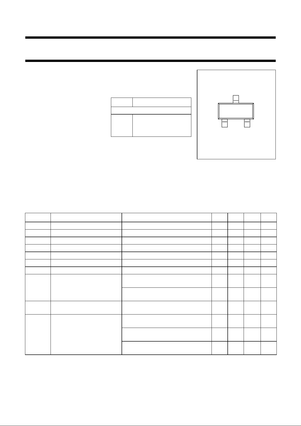
PINNING
PIN DESCRIPTION
Code: N29
page
3
1 base
DESCRIPTION
The BFR540 is an npn silicon planar
2 emitter
3 collector
12
Top view
MSB003
epitaxial transistor, intended for
applications in the RF frontend in
wideband applications in the GHz
Fig.1 SOT23.
range, such as analog and digital
cellular telephones, cordless
telephones (CT1, CT2, DECT, etc.),
radar detectors, satellite TV tuners
(SATV), MATV/CATV amplifiers and
repeater amplifiers in fibre-optic
systems.
QUICK REFERENCE DATA
SYMBOL PARAMETER CONDITIONS MIN. TYP. MAX. UNIT
V
CBO
V
CES
I
C
P
tot
h
FE
C
re
f
T
G
UM
S
21
F noise figure Γ
collector-base voltage open emitter −−20 V
collector-emitter voltage RBE=0 −−15 V
DC collector current −−120 mA
total power dissipation up to Ts = 70 °C; note 1 −−500 mW
DC current gain IC = 40 mA; VCE = 8 V 60 120 250
feedback capacitance IC=ic= 0; VCB= 8 V; f = 1 MHz − 0.6 − pF
transition frequency IC = 40 mA; VCE = 8 V; f = 1 GHz − 9 − GHz
maximum unilateral
power gain
2
insertion power gain IC = 40 mA; VCE = 8 V;
IC = 40 mA; VCE = 8 V;
T
= 25 °C; f = 900 MHz
amb
= 40 mA; VCE = 8 V;
I
C
T
= 25 °C; f = 2 GHz
amb
T
= 25 °C; f = 900 MHz
amb
T
Γ
T
Γ
T
s
amb
s
amb
s
amb
= Γ
= Γ
= Γ
= 10 mA; VCE= 8 V;
opt;IC
=25°C; f = 900 MHz
= 40 mA; VCE= 8 V;
opt;IC
=25°C; f = 900 MHz
= 10 mA; VCE= 8 V;
opt;IC
=25°C; f = 2 GHz
− 14 − dB
− 7 − dB
12 13 − dB
− 1.3 1.8 dB
− 1.9 2.4 dB
− 2.1 − dB
Note
is the temperature at the soldering point of the collector tab.
1. T
s
1999 Aug 23 2
Page 3

Philips Semiconductors Product specification
NPN 9 GHz wideband transistor BFR540
LIMITING VALUES
In accordance with the Absolute Maximum System (IEC 134).
SYMBOL PARAMETER CONDITIONS MIN. MAX. UNIT
V
CBO
V
CES
V
EBO
I
C
P
tot
T
stg
T
j
THERMAL RESISTANCE
SYMBOL PARAMETER CONDITIONS THERMAL RESISTANCE
R
th j-s
collector-base voltage open emitter − 20 V
collector-emitter voltage RBE=0 − 15 V
emitter-base voltage open collector − 2.5 V
DC collector current − 120 mA
total power dissipation up to Ts=70°C; note 1 − 500 mW
storage temperature −65 150 °C
junction temperature − 175 °C
from junction to soldering point see note 1 260 K/W
Note
is the temperature at the soldering point of the collector tab.
1. T
s
1999 Aug 23 3
Page 4

Philips Semiconductors Product specification
NPN 9 GHz wideband transistor BFR540
CHARACTERISTICS
Tj = 25 °C unless otherwise specified.
SYMBOL PARAMETER CONDITIONS MIN. TYP. MAX. UNIT
I
CBO
h
FE
C
e
C
c
C
re
f
T
G
UM
S
21
F noise figure Γ
P
L1
ITO third order intercept point note 2 − 34 − dBm
V
o
collector cut-off current IE = 0; VCB = 8 V −−50 nA
DC current gain IC= 40 mA; VCE = 8 V 60 120 250
emitter capacitance IC = ic= 0; VEB = 0.5 V; f = 1 MHz − 2 − pF
collector capacitance IE=ie= 0; VCB= 8 V; f = 1 MHz − 0.9 − pF
feedback capacitance IC= 0; VCB= 8 V; f = 1 MHz − 0.6 − pF
transition frequency IC = 40 mA; VCE = 8 V; f = 1 GHz − 9 − GHz
maximum unilateral
power gain (note 1)
2
insertion power gain IC = 40 mA; VCE = 8 V;
output power at 1 dB gain
compression
output voltage (note 3) IC= 40 mA; VCE=8 V;
IC = 40 mA; VCE = 8 V;
T
= 25 °C; f = 900 MHz
amb
= 40 mA; VCE = 8 V;
I
C
= 25 °C; f = 2 GHz
T
amb
T
= 25 °C; f = 900 MHz
amb
T
Γ
T
Γ
T
= Γ
s
amb
= Γ
s
amb
= Γ
s
amb
= 10 mA; VCE= 8 V;
opt;IC
=25°C; f = 900 MHz
= 40 mA; VCE= 8 V;
opt;IC
=25°C; f = 900 MHz
= 10 mA; VCE= 8 V;
opt;IC
=25°C; f = 2 GHz
IC= 40 mA; VCE=8 V;RL=50Ω;
T
=25°C; f = 900 MHz
amb
ZL=ZS=75Ω;T
amb
=25°C
− 14 − dB
− 7 − dB
12 13 − dB
− 1.3 1.8 dB
− 1.9 2.4 dB
− 2.1 − dB
− 21 − dBm
− 550 − mV
Notes
1. G
2. I
is the maximum unilateral power gain, assuming S12 is zero and
UM
----------------------------------------------------------
1S
–()1S
T
G
C
amb
10
UM
= 40 mA; VCE=8 V;RL=50Ω;
=25°C; f = 900 MHz;
2
S
21
2
11
–()
dB.log=
2
22
fp = 900 MHz; fq= 902 MHz;
measured at f
= 898 MHz and f
(2p−q)
(2q−p)
= 904 MHz.
3. dim= −60 dB (DIN 45004B);
Vp=VO;Vq=VO−6 dB; fp= 795.25 MHz;
VR=VO−6 dB; fq= 803.25 MHz; fr= 805.25 MHz;
measured at f
= 793.25 MHz; preliminary data.
(p+q-r)
1999 Aug 23 4
Page 5
Philips Semiconductors Product specification
NPN 9 GHz wideband transistor BFR540
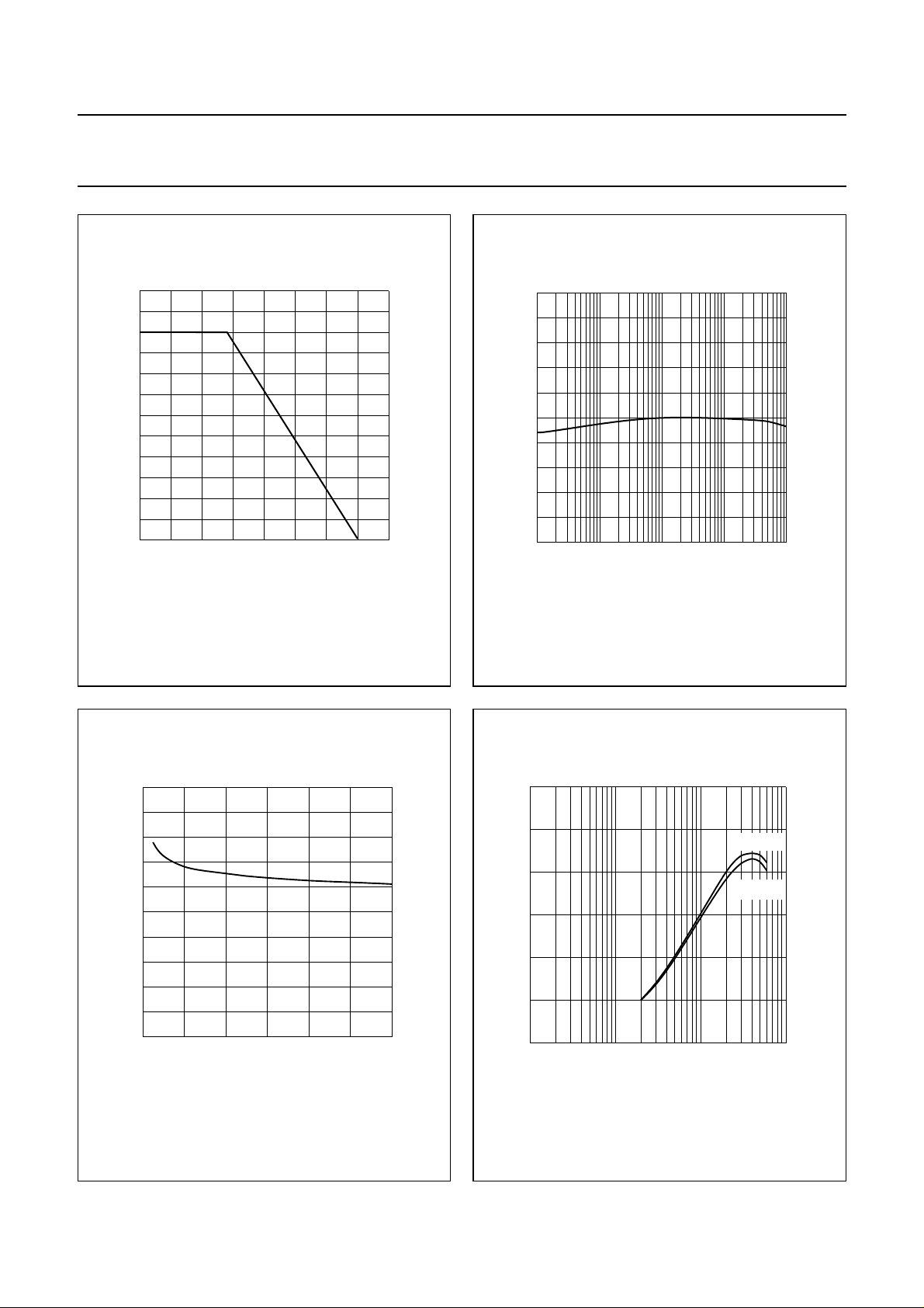
600
1/2 page (Datasheet)
P
tot
(mW)
400
200
0
0 50 100 200
Fig.2 Power derating curve.
150
MEA398 - 1
o
T ( C)
s
22 mm
10
MRA687
IC (mA)
250
handbook, halfpage
h
FE
200
150
100
50
0
−2
10
VCE= 8 V.
−1
10
1
Fig.3 DC current gain as a function of collector
current.
2
10
1.0
handbook, halfpage
C
re
(pF)
0.8
0.6
0.4
0.2
0
04812
IC = 0; f = 1 MHz.
MRA688
VCB (V)
Fig.4 Feedback capacitance as a function of
collector-base voltage.
1999 Aug 23 5
12
handbook, halfpage
f
T
(GHz)
8
4
0
−1
10
T
=25°C; f = 1 GHz.
amb
11010
IC (mA)
Fig.5 Transition frequency as a function of
collector current.
MRA689
V
= 8V
CE
VCE = 4V
2
Page 6

Philips Semiconductors Product specification
NPN 9 GHz wideband transistor BFR540
In Figs 6 to 9, GUM= maximum unilateral power gain;
MSG = maximum stable gain; G
gain.
= maximum available
max
25
handbook, halfpage
gain
(dB)
20
MSG
15
10
5
0
020
VCE= 8 V; f = 900 MHz.
G
max
G
UM
40 60
Fig.6 Gain as a function of collector current.
MRA690
I
(mA)
C
25
handbook, halfpage
gain
(dB)
20
15
10
5
0
020
VCE= 8 V; f = 2 GHz.
G
max
G
UM
40 60
Fig.7 Gain as a function of collector current.
MRA691
I
(mA)
C
G
max
f (MHz)
MRA692
4
10
50
handbook, halfpage
gain
(dB)
G
40
MSG
30
20
10
0
10
VCE= 8 V; Ic= 10 mA.
UM
2
10
3
10
Fig.8 Gain as a function of frequency.
1999 Aug 23 6
50
handbook, halfpage
gain
(dB)
G
40
MSG
30
20
10
0
10
VCE= 8 V; Ic= 40 mA.
Fig.9 Gain as a function of frequency.
UM
MRA693
G
max
2
10
3
10
f (MHz)
4
10
Page 7

Philips Semiconductors Product specification
NPN 9 GHz wideband transistor BFR540
handbook, halfpage
5
F
min
(dB)
4
3
2
1
0
VCE= 8 V.
1
2000 MHz
1000 MHz
900 MHz
500 MHz
f = 900 MHz
1000 MHz
G
ass
F
min
10
2000 MHz
IC (mA)
Fig.10 Minimum noise figure and associated
available gain as functions of collector
current.
MRA698
20
G
ass
(dB)
15
10
5
0
−5
2
10
handbook, halfpage
5
F
min
(dB)
4
3
2
1
0
10
VCE= 8 V.
IC = 10 mA
40 mA
10 mA
2
40 mA
G
ass
F
min
3
10
f (MHz)
MRA699
20
G
ass
(dB)
15
10
5
0
−5
4
10
Fig.11 Minimum noise figure and associated
available gain as functions of frequency.
handbook, full pagewidth
Zo=50Ω.
VCE= 8V; IC= 10 mA; f = 900 MHz.
pot. unst.
region
180°
stability
circle
135°
0.2
0
0.2
−135°
90°
1
0.5
F
= 1.3 dB
min
Γ
OPT
0.2 0.5
F = 1.5 dB
F = 2 dB
F = 3 dB
0.5
1 2 5
1
−90°
Fig.12 Noise circle figure.
1.0
45°
2
5
5
2
−45°
MRA700
0.8
0.6
0.4
0.2
0°
0
1.0
1999 Aug 23 7
Page 8

Philips Semiconductors Product specification
NPN 9 GHz wideband transistor BFR540
handbook, full pagewidth
Zo=50Ω.
VCE= 8 V; IC= 10 mA; f = 2000MHz.
180°
90°
1
G
135°
max
0
−135°
0.5
G = 5 dB
= 2.1 dB
Γ
OPT
F = 2.5 dB
G = 6 dB
F = 3 dB
F = 4 dB
1
−90°
G = 7 dB
= 7.8 dB
Γ
MS
0.2 0.5 1 2 5
F
min
0.2
0.5
Fig.13 Noise circle figure.
1.0
45°
2
5
5
2
−45°
MRA701
0.8
0.6
0.4
0.2
0°
0
1.0
1999 Aug 23 8
Page 9

Philips Semiconductors Product specification
NPN 9 GHz wideband transistor BFR540
handbook, full pagewidth
VCE= 8 V; IC= 40 mA.
Zo=50Ω.
90°
1
180°
135°
0.2
0
0.2
−135°
0.5
3 GHz
0.2 0.5
0.5
1 2 5
40 MHz
1
−90°
45°
2
2
−45°
Fig.14 Common emitter input reflection coefficient (S11).
5
5
MRA694
1.0
0.8
0.6
0.4
0.2
0°
0
1.0
handbook, full pagewidth
VCE= 8 V; IC= 40 mA.
90°
135°
40 MHz
180°
50 40 30 20 10
−135°
3 GHz
−90°
45°
0°
−45°
MRA695
Fig.15 Common emitter forward transmission coefficient (S21).
1999 Aug 23 9
Page 10

Philips Semiconductors Product specification
NPN 9 GHz wideband transistor BFR540
handbook, full pagewidth
VCE= 8 V; IC= 40 mA.
90°
135°
180°
0.5 0.4 0.3 0.2
−135°
3 GHz
40 MHz
0.1
−90°
45°
0°
−45°
MRA696
Fig.16 Common emitter reverse transmission coefficient (S12).
handbook, full pagewidth
VCE= 8 V; IC= 40 mA.
Zo=50Ω.
90°
1
180°
135°
0
−135°
0.5
0.2
0.2 0.5 1 2 5
3 GHz
0.2
0.5
1
−90°
2
40 MHz
2
45°
5
5
−45°
MRA697
Fig.17 Common emitter output reflection coefficient (S22).
1.0
0.8
0.6
0.4
0.2
0°
0
1.0
1999 Aug 23 10
Page 11

Philips Semiconductors Product specification
NPN 9 GHz wideband transistor BFR540
PACKAGE OUTLINE
Plastic surface mounted package; 3 leads SOT23
D
3
A
A
1
12
e
1
b
p
e
w M
B
E
H
E
detail X
AB
Q
L
p
X
v M
A
c
0 1 2 mm
scale
DIMENSIONS (mm are the original dimensions)
A
1
0.1
b
cD
p
0.48
0.15
3.0
0.38
0.09
IEC JEDEC EIAJ
2.8
1.4
1.2
e
E
1.9
REFERENCES
0.95
e
1
UNIT
mm
VERSION
A
1.1
0.9
OUTLINE
SOT23
max.
1999 Aug 23 11
H
2.5
2.1
L
Qwv
p
E
0.55
0.45
0.15
0.45
0.2
0.1
EUROPEAN
PROJECTION
ISSUE DATE
97-02-28
Page 12

Philips Semiconductors Product specification
NPN 9 GHz wideband transistor BFR540
DEFINITIONS
Data Sheet Status
Objective specification This data sheet contains target or goal specifications for product development.
Preliminary specification This data sheet contains preliminary data; supplementary data may be published later.
Product specification This data sheet contains final product specifications.
Limiting values
Limiting values given are in accordance with the Absolute Maximum Rating System (IEC 134). Stress above one or
more of the limiting values may cause permanent damage to the device. These are stress ratings only and operation
of the device at these or at any other conditions above those given in the Characteristics sections of the specification
is not implied. Exposure to limiting values for extended periods may affect device reliability.
Application information
Where application information is given, it is advisory and does not form part of the specification.
LIFE SUPPORT APPLICATIONS
These products are not designed for use in life support appliances, devices, or systems where malfunction of these
products can reasonably be expected to result in personal injury. Philips customers using or selling these products for
use in such applications do so at their own risk and agree to fully indemnify Philips for any damages resulting from such
improper use or sale.
1999 Aug 23 12
Page 13

Philips Semiconductors Product specification
NPN 9 GHz wideband transistor BFR540
NOTES
1999 Aug 23 13
Page 14

Philips Semiconductors Product specification
NPN 9 GHz wideband transistor BFR540
NOTES
1999 Aug 23 14
Page 15

Philips Semiconductors Product specification
NPN 9 GHz wideband transistor BFR540
NOTES
1999 Aug 23 15
Page 16

Philips Semiconductors – a w orldwide compan y
Argentina: see South America
Australia: 3 Figtree Drive, HOMEBUSH, NSW 2140,
Tel. +61 2 9704 8141, Fax. +61 2 9704 8139
Austria: Computerstr. 6, A-1101 WIEN, P.O. Box 213,
Tel. +43 1 60 101 1248, Fax. +43 1 60 101 1210
Belarus: Hotel Minsk Business Center, Bld. 3, r. 1211, Volodarski Str. 6,
220050 MINSK, Tel. +375 172 20 0733, Fax. +375 172 20 0773
Belgium: see The Netherlands
Brazil: see South America
Bulgaria: Philips Bulgaria Ltd., Energoproject, 15th floor,
51 James Bourchier Blvd., 1407 SOFIA,
Tel. +359 2 68 9211, Fax. +359 2 68 9102
Canada: PHILIPS SEMICONDUCTORS/COMPONENTS,
Tel. +1 800 234 7381, Fax. +1 800 943 0087
China/Hong Kong: 501 Hong Kong Industrial Technology Centre,
72 Tat Chee Avenue, Kowloon Tong, HONG KONG,
Tel. +852 2319 7888, Fax. +852 2319 7700
Colombia: see South America
Czech Republic: see Austria
Denmark: Sydhavnsgade 23, 1780 COPENHAGEN V,
Tel. +45 33 29 3333, Fax. +45 33 29 3905
Finland: Sinikalliontie 3, FIN-02630 ESPOO,
Tel. +358 9 615 800, Fax. +358 9 6158 0920
France: 51 Rue Carnot, BP317, 92156 SURESNES Cedex,
Tel. +33 1 4099 6161, Fax. +33 1 4099 6427
Germany: Hammerbrookstraße 69, D-20097 HAMBURG,
Tel. +49 40 2353 60, Fax. +49 40 2353 6300
Hungary: see Austria
India: Philips INDIA Ltd, Band Box Building, 2nd floor,
254-D, Dr. Annie Besant Road, Worli, MUMBAI 400 025,
Tel. +91 22 493 8541, Fax. +91 22 493 0966
Indonesia: PT Philips DevelopmentCorporation, Semiconductors Division,
Gedung Philips, Jl. Buncit Raya Kav.99-100, JAKARTA 12510,
Tel. +62 21 794 0040 ext. 2501, Fax. +62 21 794 0080
Ireland: Newstead, Clonskeagh, DUBLIN 14,
Tel. +353 1 7640 000, Fax. +353 1 7640 200
Israel: RAPAC Electronics, 7 Kehilat Saloniki St, PO Box 18053,
TEL AVIV 61180, Tel. +972 3 645 0444, Fax. +972 3 649 1007
Italy: PHILIPS SEMICONDUCTORS, Via Casati, 23 - 20052 MONZA (MI),
Tel. +39 039 203 6838, Fax +39 039 203 6800
Japan: Philips Bldg 13-37, Kohnan 2-chome, Minato-ku,
TOKYO 108-8507, Tel. +81 3 3740 5130, Fax. +81 3 3740 5057
Korea: Philips House, 260-199 Itaewon-dong, Yongsan-ku, SEOUL,
Tel. +82 2 709 1412, Fax. +82 2 709 1415
Malaysia: No. 76 Jalan Universiti, 46200 PETALING JAYA, SELANGOR,
Tel. +60 3 750 5214, Fax. +60 3 757 4880
Mexico: 5900 Gateway East, Suite 200, EL PASO, TEXAS 79905,
Tel. +9-5 800 234 7381, Fax +9-5 800 943 0087
Middle East: see Italy
Netherlands: Postbus 90050, 5600 PB EINDHOVEN, Bldg. VB,
Tel. +31 40 27 82785, Fax. +31 40 27 88399
New Zealand: 2 Wagener Place, C.P.O. Box 1041, AUCKLAND,
Tel. +64 9 849 4160, Fax. +64 9 849 7811
Norway: Box 1, Manglerud 0612, OSLO,
Tel. +47 22 74 8000, Fax. +47 22 74 8341
Pakistan: see Singapore
Philippines: Philips Semiconductors Philippines Inc.,
106 Valero St. Salcedo Village, P.O. Box 2108 MCC, MAKATI,
Metro MANILA, Tel. +63 2 816 6380, Fax. +63 2 817 3474
Poland: Ul. Lukiska 10, PL 04-123 WARSZAWA,
Tel. +48 22 612 2831, Fax. +48 22 612 2327
Portugal: see Spain
Romania: see Italy
Russia: Philips Russia, Ul. Usatcheva 35A, 119048 MOSCOW,
Tel. +7 095 755 6918, Fax. +7 095 755 6919
Singapore: Lorong 1, Toa Payoh, SINGAPORE 319762,
Tel. +65 350 2538, Fax. +65 251 6500
Slovakia: see Austria
Slovenia: see Italy
South Africa: S.A. PHILIPS Pty Ltd., 195-215 Main Road Martindale,
2092 JOHANNESBURG, P.O. Box 58088 Newville 2114,
Tel. +27 11 471 5401, Fax. +27 11 471 5398
South America: Al. Vicente Pinzon, 173, 6th floor,
04547-130 SÃO PAULO, SP, Brazil,
Tel. +55 11 821 2333, Fax. +55 11 821 2382
Spain: Balmes 22, 08007 BARCELONA,
Tel. +34 93 301 6312, Fax. +34 93 301 4107
Sweden: Kottbygatan 7, Akalla, S-16485 STOCKHOLM,
Tel. +46 8 5985 2000, Fax. +46 8 5985 2745
Switzerland: Allmendstrasse 140, CH-8027 ZÜRICH,
Tel. +41 1 488 2741 Fax. +41 1 488 3263
Taiwan: Philips Semiconductors, 6F, No. 96, Chien Kuo N. Rd., Sec. 1,
TAIPEI, Taiwan Tel. +886 2 2134 2886, Fax. +886 2 2134 2874
Thailand: PHILIPS ELECTRONICS (THAILAND) Ltd.,
209/2 Sanpavuth-Bangna Road Prakanong, BANGKOK 10260,
Tel. +66 2 745 4090, Fax. +66 2 398 0793
Turkey: Yukari Dudullu, Org. San. Blg., 2.Cad. Nr. 28 81260 Umraniye,
ISTANBUL, Tel. +90 216 522 1500, Fax. +90 216 522 1813
Ukraine: PHILIPS UKRAINE, 4 Patrice Lumumba str., Building B, Floor 7,
252042 KIEV, Tel. +380 44 264 2776, Fax. +380 44 268 0461
United Kingdom: Philips Semiconductors Ltd., 276 Bath Road, Hayes,
MIDDLESEX UB3 5BX, Tel. +44 208 730 5000, Fax. +44 208 754 8421
United States: 811 East Arques Avenue, SUNNYVALE, CA 94088-3409,
Tel. +1 800 234 7381, Fax. +1 800 943 0087
Uruguay: see South America
Vietnam: see Singapore
Yugoslavia: PHILIPS, Trg N. Pasica 5/v, 11000 BEOGRAD,
Tel. +381 11 62 5344, Fax.+381 11 63 5777
For all other countries apply to: Philips Semiconductors,
International Marketing & Sales Communications, Building BE-p, P.O. Box 218,
5600 MD EINDHOVEN, The Netherlands, Fax. +31 40 27 24825
© Philips Electronics N.V. SCA
All rights are reserved. Reproduction in whole or in part is prohibited without the prior written consent of the copyright owner.
The information presented in this document does not form part of any quotation or contract, is believed to be accurate and reliable and may be changed
without notice. No liability will be accepted by the publisher for any consequence of its use. Publication thereof does not convey nor imply any license
under patent- or other industrial or intellectual property rights.
1999
Internet: http://www.semiconductors.philips.com
67
Printed in The Netherlands 125006/03/pp16 Date of release: 1999 Aug 23 Document order number: 9397 750 06338
 Loading...