

NPN Silicon RF Transistor BFQ 71
● For broadband amplifiers up to 2 GHz and fast
non-saturated switches at collector currents from
1 mA to 20 mA.
● Hermetically sealed ceramic package.
● HiRel/Mil screening available.
● CECC-type available: CECC 50002/260.
ESD: Electrostatic discharge sensitive device, observe handling precautions!
Type Ordering Code
Marking
(tape and reel)
BFQ 71 Q62702-F77571 Cerec-X
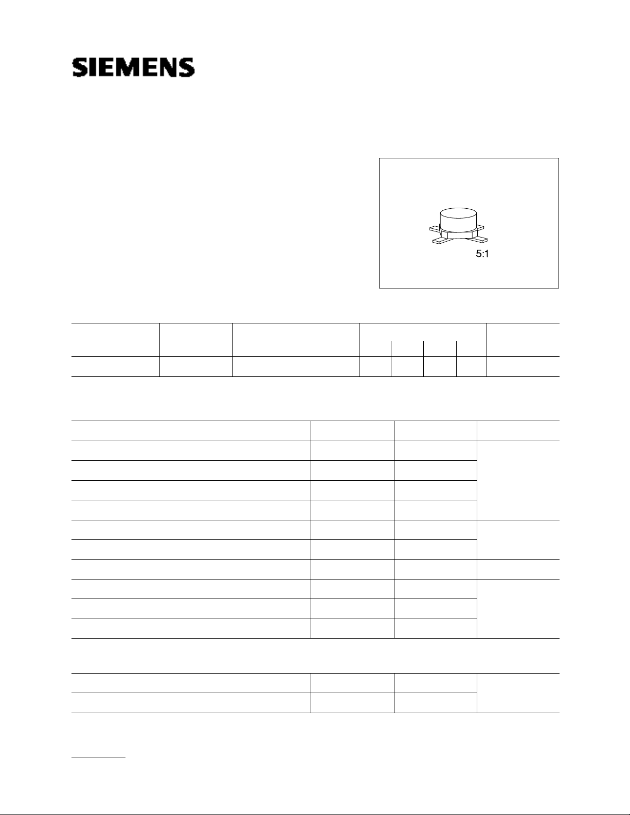
Pin Configuration
1 2 3
B E C
Package
4
E
Maximum Ratings
Parameter Symbol Values Unit
Collector-emitter voltage V
CE0 15 V
Collector-emitter voltage, VBE = 0 VCES 20
Collector-base voltage V
CB0 20
Emitter-base voltage VEB0 2.5
Collector current I
C 30 mA
Base current IB 4
Total power dissipation, T
S ≤ 103 ˚C
3)
Ptot 300 mW
Junction temperature Tj 175 ˚C
1)
Ambient temperature range T
Storage temperature range T
A – 65 … + 175
stg – 65 … + 175
Thermal Resistance
Junction - ambient
Junction - soldering point
1)
For detailed dimensions see chapter Package Outlines.
2)
Package mounted on alumina 15 mm× 16.7 mm × 0.7 mm.
3)
TS is measured on the collector lead at the soldering point to the pcb.
2)
3)
Rth JA ≤ 320 K/W
Rth JS ≤ 240
Electrical Characteristics
A = 25 ˚C, unless otherwise specified.
at T
BFQ 71
Parameter Symbol
DC Characteristics
V
(BR)CE0 15 – –
C = 1 mA, IB = 0
I
I
CB0 ––50
CB = 10 V, IE = 0
V
I
EB0 ––10
EB = 2 V, IC = 0
V
FE
h
IC = 5 mA, VCE = 6 V
C = 20 mA, VCE = 6 V
I
V
CEsat – 0.16 0.4
C = 30 mA, IB = 3 mA
I
Base-emitter voltage
C = 5 mA, VCE = 6 V
I
V
BE – 0.78 –
min. typ. max.
40
40
90
100
250
–
UnitValues
VCollector-emitter breakdown voltage
nACollector-base cutoff current
µAEmitter-base cutoff current
–DC current gain
VCollector-emitter saturation voltage
Electrical Characteristics
A = 25 ˚C, unless otherwise specified.
at T
BFQ 71
Parameter Symbol
AC Characteristics
T
f
C = 5 mA, VCE = 6 V, f = 200 MHz
I
C = 20 mA, VCE = 6 V, f = 200 MHz
I
C
cb – 0.46 0.6
CB = 6 V, VBE = vbe = 0, f = 1 MHz
V
C
Collector-emitter capacitance
CE = 6 V, VBE = vbe = 0, f = 1 MHz
V
Input capacitance
EB = 0.5 V, IC = ic = 0, f = 1 MHz
V
Output capacitance
CE = 6 V, VBE = vbe = 0, f = 1 MHz
V
ce – 0.4 –
C
ibo – 1.2 –
C
obs – 0.86 1.2
F
I
C = 5 mA, VCE = 6 V, f = 10 MHz, ZS = 75 Ω
C = 2 mA, VCE = 6 V, f = 800 MHz, ZS = ZSopt
I
IC = 3 mA, VCE = 10 V, f = 2 GHz, ZS = ZSopt
min. typ. max.
–
4
–
–
–
4.2
5.2
1.4
1.5
3.2
–
–
2.2
3
–
UnitValues
GHzTransition frequency
pFCollector-base capacitance
dBNoise figure
Power gain
C = 2 mA, VCE = 6 V, f = 800 MHz,
I
S = ZSopt, ZL = ZLopt
Z
Transducer gain
C = 20 mA, VCE = 6 V, f = 1 GHz, Z0 = 50 Ω
I
two-tone intermodulation test
C = 15 mA, VCE = 10 V, dIM = 60 dB,
I
1 = 806 MHz, f2 = 810 MHz, ZS = ZL = 50 Ω
f
C = 15 mA, VCE = 10 V, f = 800 MHz
I
Gpe –15–
2
I S
21e I
– 13.4 –
Vo1 = Vo2 – 110 –
IP
3 – 23.5 –
mVLinear output voltage
dBmThird order intercept point
BFQ 71
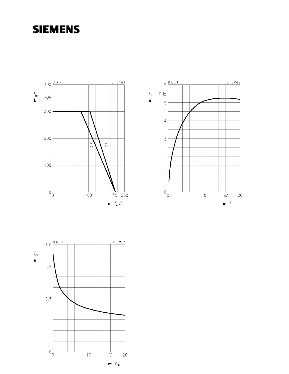
Total power dissipation Ptot = f (TA*; TS)
*Package mounted on alumina
Transition frequency fT = f (IC)
CE = 6 V, f = 200 MHz
V
Collector-base capacitance C
BE = vbe = 0, f = 1 MHz
V
cb = f (VCB)
BFQ 71
Common Emitter Noise Parameters
Γ
f
Fmin Gp(Fmin) RN NF50 Ω Gp(F50Ω)
GHz dB dB MAG ANG Ω –dBdB
IC = 2 mA, VCE = 6 V, Z0 = 50 Ω
opt
0.01 1.1 – (Z
IC = 5 mA, VCE = 10 V, Z0 = 50 Ω
0.01
0.8
2.0
1.3
1.6
3.1
–
15.3
9
0.29
0.12
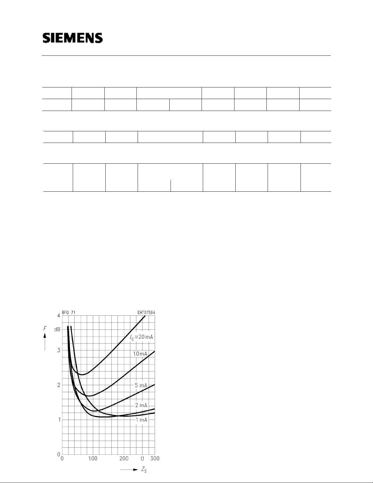
Noise figure F = f (ZS)
CE = 6 V, f = 10 MHz
V
S = 150 Ω) – – 1.6 –
S = 100 Ω)
(Z
56
124.5
–
18.5
30
–
0.24
0.67
1.7
1.8
–
–
14.8
–
BFQ 71
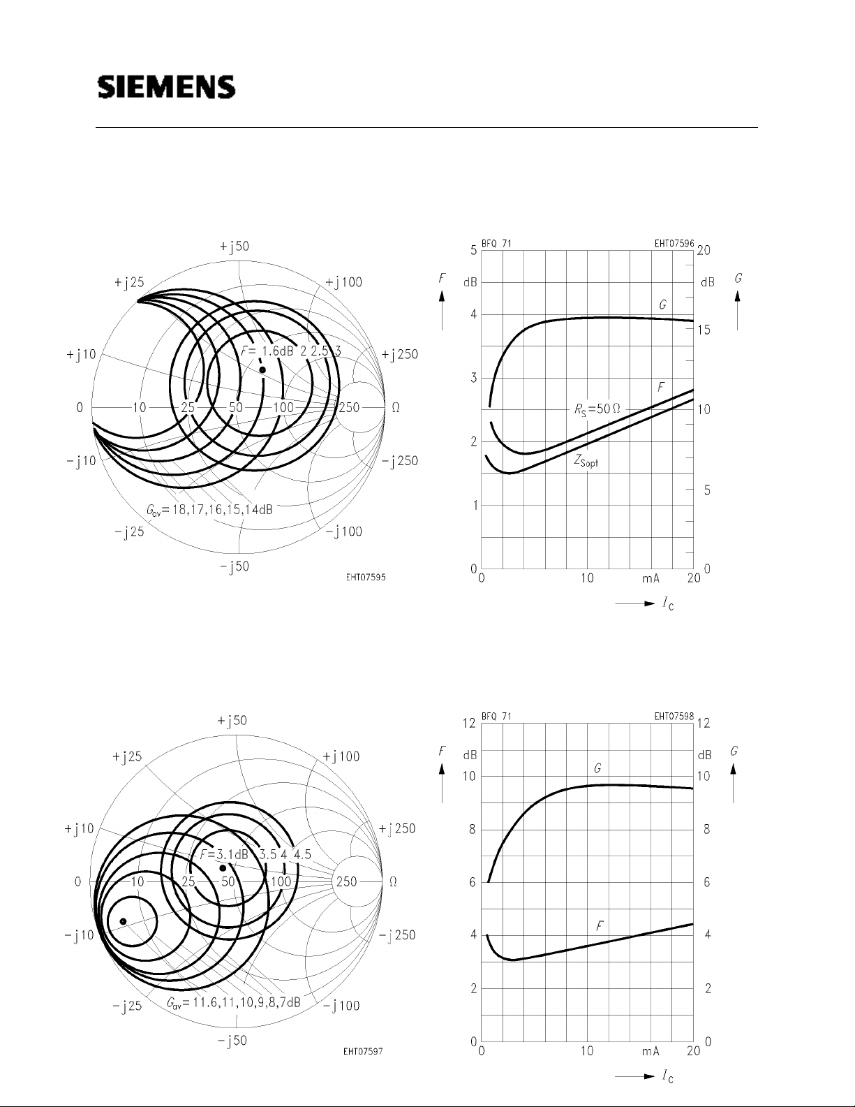
Circles of constant noise figure F = f (ZS)
and available power gain G
C = 5 mA, VCE = 10 V, f = 800 MHz
I
av = f (ZS)
Noise figure F = f (IC)
Power gain G = f (I
CE = 10 V, f = 800 MHz, ZLopt (G)
V
C)
Circles of constant noise figure F = f (Z
and available power gain G
C = 5 mA, VCE = 10 V, f = 2 GHz
I
av = f (ZS)
Noise figure F = f (I
S)
Power gain G = f (I
CE = 10 V, f = 2 GHz, ZLopt (G)
V
C)
C)

Common Emitter Power Gain
BFQ 71
Power gain G
CE = 6 V, f = 200 MHz, Z0 = 50 Ω
V
ms, S21e
2
= f (IC)
Power gain Gms, S21e 2 = f (IC)
CE = 6 V, f = 500 MHz, Z0 = 50 Ω
V
Power gain G
CE = 6 V, f = 800 MHz, Z0 = 50 Ω
V
ms, S21e
2
= f (IC)
Power gain G
CE = 6 V, f = 2 GHz, Z0 = 50 Ω
V
ma, S21e
2
= f (IC)

BFQ 71
Power gain Gms, S21e 2 = f (f)
C = 2 mA, VCE = 6 V, Z0 = 50 Ω
I
Power gain Gma,Gms, S21e 2 = f (f)
C = 5 mA, VCE = 6 V, Z0 = 50 Ω
I
Power gain G
C = 10 mA, VCE = 6 V, Z0 = 50 Ω
I
ma, Gms, S21e
2
= f (f)
Power gain G
C = 20 mA, VCE = 6 V, Z0 = 50 Ω
I
ma, Gms, S21e
2
= f (f)

Common Emitter S Parameters
BFQ 71
fS
11 S21 S12 S22
GHz MAG ANG MAG ANG MAG ANG MAG ANG
IC = 2 mA, VCE = 6 V, Z0 = 50 Ω
0.1
0.2
0.3
0.4
0.6
0.8
1.0
1.2
1.5
1.8
2.0
2.5
3.0
0.90
0.87
0.81
0.77
0.69
0.64
0.61
0.59
0.57
0.57
0.58
0.59
0.60
– 19
– 37
– 55
– 71
– 97
– 118
– 134
– 147
– 163
– 176
176
159
145
6.93
6.45
5.85
5.41
4.41
3.64
3.06
2.64
2.19
1.87
1.70
1.41
1.21
166
152
140
129
112
98
87
79
66
56
49
34
21
0.025
0.048
0.068
0.082
0.101
0.112
0.118
0.121
0.125
0.129
0.131
0.138
0.150
78
68
59
51
40
33
28
25
22
20
20
20
19
0.98
0.94
0.88
0.82
0.73
0.65
0.60
0.57
0.54
0.52
0.51
0.49
0.48
– 8
– 16
– 23
– 28
– 36
– 41
– 45
– 49
– 54
– 60
– 65
– 78
– 92
S11, S22 = f (f)
C = 2 mA, VCE = 6 V, Z0 = 50 Ω
I
S12, S21 = f (f)
C = 2 mA, VCE = 6 V, Z0 = 50 Ω
I

Common Emitter S Parameters (continued)
BFQ 71
fS
11 S21 S12 S22
GHz MAG ANG MAG ANG MAG ANG MAG ANG
IC = 5 mA, VCE = 6 V, Z0 = 50 Ω
0.1
0.2
0.3
0.4
0.6
0.8
1.0
1.2
1.5
1.8
2.0
2.5
3.0
0.79
0.73
0.66
0.62
0.57
0.55
0.54
0.54
0.54
0.54
0.56
0.57
0.59
– 31
– 59
– 83
– 102
– 128
– 146
– 160
– 170
178
168
162
148
136
14.23
12.37
10.36
8.88
6.56
5.12
4.17
3.55
2.89
2.43
2.20
1.81
1.55
160
151
127
115
100
89
80
73
63
54
48
35
23
0.023
0.040
0.053
0.060
0.071
0.077
0.083
0.089
0.099
0.110
0.117
0.137
0.158
76
61
51
45
40
37
37
37
37
37
36
35
32
0.95
0.84
0.73
0.65
0.53
0.47
0.43
0.40
0.38
0.37
0.36
0.34
0.34
– 14
– 26
– 33
– 38
– 43
– 46
– 48
– 51
– 55
– 61
– 65
– 78
– 92
S11, S22 = f (f)
C = 5 mA, VCE = 6 V, Z0 = 50 Ω
I
S12, S21 = f (f)
C = 5 mA, VCE = 6 V, Z0 = 50 Ω
I

Common Emitter S Parameters (continued)
BFQ 71
fS
11 S21 S12 S22
GHz MAG ANG MAG ANG MAG ANG MAG ANG
IC = 10 mA, VCE = 6 V, Z0 = 50 Ω
0.1
0.2
0.3
0.4
0.6
0.8
1.0
1.2
1.5
1.8
2.0
2.5
3.0
0.68
0.60
0.55
0.55
0.53
0.53
0.53
0.53
0.53
0.54
0.56
0.58
0.60
– 47
– 85
– 111
– 128
– 150
– 164
– 174
178
168
160
155
143
132
22.06
17.31
13.39
10.84
7.60
5.80
4.67
3.95
3.19
2.67
2.42
1.99
1.69
152
130
116
106
93
83
76
70
60
52
47
34
23
0.020
0.032
0.040
0.045
0.053
0.061
0.069
0.078
0.091
0.106
0.114
0.138
0.163
70
56
49
46
46
46
47
48
48
47
46
43
38
0.90
0.73
0.59
0.51
0.41
0.37
0.34
0.32
0.31
0.31
0.30
0.28
0.28
– 20
– 33
– 39
– 42
– 44
– 46
– 47
– 49
– 53
– 59
– 63
– 76
– 91
S11, S22 = f (f)
C = 10 mA, VCE = 6 V, Z0 = 50 Ω
I
S12, S21 = f (f)
C = 10 mA, VCE = 6 V, Z0 = 50 Ω
I

Common Emitter S Parameters (continued)
BFQ 71
fS
11 S21 S12 S22
GHz MAG ANG MAG ANG MAG ANG MAG ANG
IC = 15 mA, VCE = 6 V, Z0 = 50 Ω
0.1
0.2
0.3
0.4
0.6
0.8
1.0
1.2
1.5
1.8
2.0
2.5
3.0
0.56
0.47
0.42
0.42
0.41
0.40
0.41
0.41
0.41
0.43
0.44
0.46
0.50
– 57
– 96
– 121
– 137
– 156
– 168
– 177
176
169
161
156
147
137
25.74
18.17
13.28
10.48
7.19
5.46
4.39
3.71
3.01
2.53
2.31
1.91
1.65
145
122
109
100
89
81
74
68
59
52
47
35
24
0.018
0.028
0.035
0.042
0.054
0.068
0.082
0.096
0.118
0.142
0.158
0.204
0.255
69
58
56
57
59
60
60
60
58
56
53
47
38
0.85
0.65
0.54
0.47
0.41
0.39
0.37
0.36
0.35
0.35
0.34
0.33
0.32
– 23
– 32
– 35
– 35
– 36
– 37
– 39
– 41
– 45
– 52
– 57
– 70
– 88
S11, S22 = f (f)
C = 15 mA, VCE = 6 V, Z0 = 50 Ω
I
S12, S21 = f (f)
C = 15 mA, VCE = 6 V, Z0 = 50 Ω
I

Common Emitter S Parameters (continued)
BFQ 71
fS
11 S21 S12 S22
GHz MAG ANG MAG ANG MAG ANG MAG ANG
IC = 20 mA, VCE = 6 V, Z0 = 50 Ω
0.1
0.2
0.3
0.4
0.6
0.8
1.0
1.2
1.5
1.8
2.0
2.5
3.0
0.54
0.52
0.51
0.52
0.52
0.53
0.54
0.54
0.54
0.55
0.58
0.59
0.62
– 71
– 114
– 137
– 150
– 166
– 176
176
170
161
155
150
140
130
29.35
20.19
14.58
11.40
7.77
5.86
4.69
3.96
3.19
2.66
2.41
1.97
1.68
142
119
106
98
87
79
73
66
57
50
45
32
21
0.016
0.025
0.030
0.034
0.043
0.053
0.062
0.072
0.087
0.102
0.112
0.137
0.162
66
52
51
51
54
56
56
56
55
53
52
48
42
0.82
0.60
0.48
0.42
0.36
0.34
0.32
0.31
0.30
0.30
0.30
0.28
0.28
– 25
– 36
– 39
– 39
– 38
– 39
– 41
– 43
– 47
– 54
– 59
– 72
– 87
S11, S22 = f (f)
C = 20 mA, VCE = 6 V, Z0 = 50 Ω
I
S12, S21 = f (f)
C = 20 mA, VCE = 6 V, Z0 = 50 Ω
I

Common Emitter S Parameters (continued)
BFQ 71
fS
11 S21 S12 S22
GHz MAG ANG MAG ANG MAG ANG MAG ANG
IC = 2 mA, VCE = 10 V, Z0 = 50 Ω
0.1
0.2
0.3
0.4
0.6
0.8
1.0
1.2
1.5
1.8
2.0
2.5
3.0
0.91
0.87
0.82
0.78
0.70
0.64
0.60
0.58
0.56
0.56
0.57
0.58
0.59
– 17
– 36
– 53
– 69
– 94
– 115
– 132
– 145
– 161
– 174
177
160
146
7.02
6.57
5.98
5.01
4.54
3.76
3.17
2.74
2.28
1.94
1.77
1.47
1.26
166
153
141
130
113
100
89
80
68
57
51
36
22
0.021
0.042
0.060
0.073
0.090
0.100
0.106
0.109
0.113
0.118
0.120
0.127
0.140
78
69
60
53
42
35
30
27
24
23
23
23
23
0.98
0.95
0.90
0.84
0.75
0.69
0.64
0.61
0.58
0.56
0.55
0.53
0.52
– 7
– 14
– 20
– 25
– 33
– 38
– 41
– 45
– 50
– 55
– 60
– 72
– 85
S11, S22 = f (f)
C = 2 mA, VCE = 10 V, Z0 = 50 Ω
I
S12, S21 = f (f)
C = 2 mA, VCE = 10 V, Z0 = 50 Ω
I

Common Emitter S Parameters (continued)
BFQ 71
fS
11 S21 S12 S22
GHz MAG ANG MAG ANG MAG ANG MAG ANG
IC = 5 mA, VCE = 10 V, Z0 = 50 Ω
0.1
0.2
0.3
0.4
0.6
0.8
1.0
1.2
1.5
1.8
2.0
2.5
3.0
0.80
0.73
0.67
0.63
0.57
0.54
0.53
0.52
0.52
0.53
0.54
0.56
0.58
– 28
– 57
– 79
– 98
– 125
– 143
– 157
– 168
180
170
163
150
137
14.24
12.50
10.55
9.10
6.78
5.31
4.33
3.69
3.00
2.52
2.29
1.89
1.61
160
142
128
117
101
90
81
74
63
54
49
36
23
0.020
0.036
0.047
0.055
0.064
0.071
0.076
0.082
0.091
0.101
0.108
0.127
0.148
71
61
53
47
41
39
38
38
39
39
39
38
35
0.95
0.86
0.76
0.68
0.58
0.52
0.48
0.46
0.44
0.43
0.42
0.40
0.40
– 13
– 23
– 29
– 34
– 38
– 41
– 43
– 45
– 49
– 55
– 59
– 70
– 84
S11, S22 = f (f)
C = 5 mA, VCE = 10 V, Z0 = 50 Ω
I
S12, S21 = f (f)
C = 5 mA, VCE = 10 V, Z0 = 50 Ω
I

Common Emitter S Parameters (continued)
BFQ 71
fS
11 S21 S12 S22
GHz MAG ANG MAG ANG MAG ANG MAG ANG
IC = 10 mA, VCE = 10 V, Z0 = 50 Ω
0.1
0.2
0.3
0.4
0.6
0.8
1.0
1.2
1.5
1.8
2.0
2.5
3.0
0.68
0.60
0.56
0.54
0.51
0.51
0.51
0.51
0.51
0.52
0.54
0.56
0.58
– 43
– 78
– 105
– 123
– 146
– 161
– 171
180
170
162
156
145
134
21.82
17.39
13.60
11.10
7.83
5.99
4.83
4.08
3.30
2.77
2.51
2.06
1.75
153
131
117
107
94
84
77
70
61
53
48
35
23
0.018
0.030
0.037
0.042
0.050
0.057
0.064
0.072
0.084
0.098
0.106
0.129
0.152
71
58
50
47
46
47
48
49
49
48
47
45
40
0.91
0.76
0.64
0.56
0.47
0.43
0.41
0.39
0.38
0.38
0.37
0.35
0.35
– 17
– 29
– 34
– 36
– 38
– 39
– 41
– 43
– 48
– 52
– 56
– 67
– 81
S11, S22 = f (f)
C = 10 mA, VCE = 10 V, Z0 = 50 Ω
I
S12, S21 = f (f)
C = 10 mA, VCE = 10 V, Z0 = 50 Ω
I

Common Emitter S Parameters (continued)
BFQ 71
fS
11 S21 S12 S22
GHz MAG ANG MAG ANG MAG ANG MAG ANG
IC = 15 mA, VCE = 10 V, Z0 = 50 Ω
0.1
0.2
0.3
0.4
0.6
0.8
1.0
1.2
1.5
1.8
2.0
2.5
3.0
0.62
0.55
0.52
0.51
0.50
0.50
0.51
0.51
0.51
0.53
0.54
0.57
0.59
– 55
– 94
– 119
– 136
– 156
– 169
– 178
175
166
158
153
143
132
26.35
19.54
14.64
11.66
8.06
6.12
4.91
4.15
3.35
2.80
2.53
2.07
1.77
148
125
112
102
90
82
75
68
59
51
47
34
23
0.017
0.026
0.031
0.036
0.044
0.052
0.061
0.069
0.082
0.097
0.106
0.129
0.153
69
55
50
50
51
52
53
54
53
52
51
48
43
0.88
0.69
0.57
0.50
0.44
0.41
0.39
0.38
0.37
0.37
0.36
0.34
0.34
– 20
– 31
– 34
– 35
– 35
– 36
– 38
– 40
– 44
– 50
– 54
– 65
– 80
S11, S22 = f (f)
C = 15 mA, VCE = 10 V, Z0 = 50 Ω
I
S12, S21 = f (f)
C = 15 mA, VCE = 10 V, Z0 = 50 Ω
I

Common Emitter S Parameters (continued)
BFQ 71
fS
11 S21 S12 S22
GHz MAG ANG MAG ANG MAG ANG MAG ANG
IC = 20 mA, VCE = 10 V, Z0 = 50 Ω
0.1
0.2
0.3
0.4
0.6
0.8
1.0
1.2
1.5
1.8
2.0
2.5
3.0
0.57
0.52
0.50
0.51
0.50
0.51
0.52
0.52
0.52
0.53
0.55
0.57
0.60
– 63
– 106
– 130
– 144
– 162
– 173
179
172
163
156
152
141
131
28.86
20.30
14.82
11.65
7.97
6.02
4.83
4.08
3.29
2.74
2.49
2.04
1.73
144
121
108
99
88
80
73
67
58
50
46
33
22
0.015
0.024
0.029
0.033
0.041
0.050
0.058
0.068
0.081
0.096
0.104
0.128
0.152
65
54
50
52
54
56
56
57
56
54
53
50
44
0.84
0.65
0.54
0.49
0.43
0.41
0.40
0.38
0.38
0.38
0.37
0.36
0.36
– 21
– 30
– 32
– 32
– 32
– 33
– 35
– 38
– 42
– 48
– 53
– 64
– 79
S11, S22 = f (f)
C = 20 mA, VCE = 10 V, Z0 = 50 Ω
I
S12, S21 = f (f)
C = 20 mA, VCE = 10 V, Z0 = 50
I
 Loading...