

Page 1
DISCRETE SEMICONDUCTORS
DATA SH EET
BFQ621
NPN 7 GHz wideband transistor
Product specification
Supersedes data of 1995 Apr 11
File under Discrete Semiconductors, SC14
1995 Sep 26
Page 2
Philips Semiconductors Product specification
NPN 7 GHz wideband transistor BFQ621
FEATURES
• High power gain
• High output voltage
• High maximum junction temperature
• Gold metallization ensures excellent reliability.
APPLICATIONS
It is primarily intended for use in MATV and microwave
amplifiers, such as aerial amplifiers, radar systems,
oscilloscopes, spectrum analyzers, etc.
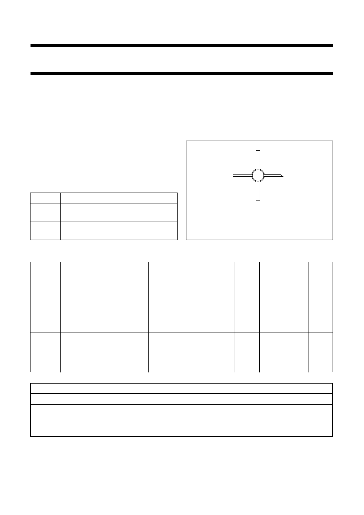
PINNING
PIN DESCRIPTION
1 collector
2 emitter
3 base
4 emitter
QUICK REFERENCE DATA
DESCRIPTION
Silicon NPN transistor in a 4-lead dual-emitter SOT172A2
package with a ceramic cap. All leads are isolated from the
mounting base. Emitter ballasting resistors and application
of gold sandwich metallization ensures an optimum
temperature profile and excellent reliability properties.
handbook, halfpage
3
Top view
4
1
2
MSA457
Fig.1 SOT172A2.
SYMBOL PARAMETER CONDITIONS MIN. TYP. MAX. UNIT
V
CEO
I
C
P
tot
h
FE
f
T
G
UM
V
O
collector-emitter voltage open base −−16 V
collector current (DC) −−150 mA
total power dissipation up to Tmb=25°C −−8W
DC current gain IC= 120 mA; VCE=18V;
T
=25°C
amb
transition frequency IC= 120 mA; VCE=18V;
f = 1 GHz; T
amb
=25°C
maximum unilateral power gain IC= 120 mA; VCE=18V;
f = 500 MHz; T
amb
=25°C
output voltage IC= 120 mA; VCE=18V;
f
(p+q−r)
= 793.25 MHz;
40 −−
− 7 − GHz
− 18.5 − dB
− 1.2 − V
dim= −60 dB; RL=75Ω
WARNING
Product and environmental safety - toxic materials
This product contains beryllium oxide. The product is entirely safe provided that the BeO disc is not damaged.
All persons who handle, use or dispose of this product should be aware of its nature and of the necessary safety
precautions. After use, dispose of as chemical or special waste according to the regulations applying at the location of
the user. It must never be thrown out with the general or domestic waste.
1995 Sep 26 2
Page 3
Philips Semiconductors Product specification
NPN 7 GHz wideband transistor BFQ621
LIMITING VALUES
In accordance with the Absolute Maximum Rating System (IEC 134).
SYMBOL PARAMETER CONDITIONS MIN. MAX. UNIT
V
CBO
V
CEO
V
EBO
I
C
P
tot
T
stg
T
j
THERMAL CHARACTERISTICS
SYMBOL PARAMETER CONDITIONS VALUE UNIT
R
th j-mb
collector-base voltage open emitter − 25 V
collector-emitter voltage open base − 16 V
emitter-base voltage open collector − 2V
collector current (DC) − 150 mA
total power dissipation up to Tmb=25°C − 8W
storage temperature −65 +175 °C
junction temperature − +200 °C
thermal resistance from junction to mounting base P
= 8 W; up to Tmb=25°C 21.9 K/W
tot
1995 Sep 26 3
Page 4

Philips Semiconductors Product specification
NPN 7 GHz wideband transistor BFQ621
CHARACTERISTICS
T
=25°C (unless otherwise specified).
j
SYMBOL PARAMETER CONDITIONS MIN. TYP. MAX. UNIT
V
(BR)CBO
V
(BR)CEO
V
(BR)EBO
I
CBO
h
FE
f
T
C
c
C
e
C
re
G
UM
V
O
d
2
collector-base breakdown voltage IC= 0.1 mA; IE=0 −−25 V
collector-emitter breakdown voltage IC= 10 mA; IB=0 −−16 V
emitter-base breakdown voltage IE= 0.1 mA; IC=0 −−2V
collector-base leakage current IE= 0; VCB=18V −−100 µA
DC current gain IC= 50 mA; VCE=10V 50 − 160
transition frequency IC= 120 mA; VCE=18V;
− 7 − GHz
f = 1 GHz; see Fig.3
collector capacitance IE=ie= 0; VCB=18V;
− 1.5 − pF
f = 1 MHz
emitter capacitance IC=ic= 0; VEB= 0.5 V;
− 5 − pF
f = 1 MHz
feedback capacitance IC= 0; VCE= 18 V; f = 1 MHz;
− 0.85 1.2 pF
see Fig.4
maximum unilateral power gain;
note 1
IC= 120 mA; VCE=18V;
f = 500 MHz; T
= 120 mA; VCE=18V;
I
C
f = 800 MHz; T
amb
amb
=25°C;
=25°C;
− 18.5 − dB
− 14.5 − dB
output voltage note 2 − 1.35 − V
note 3 − 1.2 − V
second order intermodulation
distortion
note 4 −−60 − dB
note 5 −−60 − dB
Notes
1. G
2. d
is the maximum unilateral power gain, assuming s12 is zero.
UM
= −60dB (DIN45004B); see Fig.2; IC= 120 mA; VCE= 18 V; RL=75Ω;T
im
G
UM
10
Vp=VO; fp= 445.25 MHz;
Vq=VO−6 dB; fq= 453.25 MHz;
Vr=VO−6 dB; fr= 455.25 MHz;
measured at f
(p+q−r)
= 443.25 MHz; see Fig.5.
3. dim= −60dB (DIN45004B); see Fig.2; IC= 120 mA; VCE= 18 V; RL=75Ω;T
Vp=VO; fp= 795.25 MHz;
Vq=VO−6 dB; fq= 803.25 MHz;
Vr=VO−6 dB; fr= 805.25 MHz;
measured at f
(p+q−r)
4. VO= 50 dBmV = 316 mV; IC= 90 mA; VCE= 18 V; RL=75Ω;T
measured at f
5. V
= 50 dBmV = 316 mV; IC= 90 mA; VCE= 18 V; RL=75Ω;T
O
measured at f
(p+q)
(p+q)
= 793.25 MHz; see Fig.6.
= 450 MHz; see Fig.7.
= 810 MHz; see Fig.8.
amb
amb
=25°C;
=25°C;
s
-----------------------------------------------------------1s
–()1s
=25°C;
amb
=25°C;
amb
21
2
11
2
dB.log=
2
–()
22
1995 Sep 26 4
Page 5

Philips Semiconductors Product specification
MEA260
NPN 7 GHz wideband transistor BFQ621
V
handbook, full pagewidth
V
BB
input
75 Ω
10 nF
L2
10 nF L6
10 nF
1 pF
10 kΩ
L1
L5
240 Ω
L3
DUT
33Ω 33
Ω
L4
10 nF
10 nF
MEA260
4.7 µF
CC
output
75 Ω
1 pF
L1 =8 nH.
L2 = 15 nH, 2 turns copper wire, internal diameter 2 mm.
L3 = 10 nH, 2 turns copper wire, internal diameter 1.5 mm.
L5: Lp = 21 mm; Rc = 75 Ω.
L6: Lp = 16 mm; Rc = 75 Ω.
Fig.2 Intermodulation distortion and second order distortion MATV test circuit.
10
handbook, halfpage
f
T
(GHz)
8
6
4
2
0
0 100 20050 150
MLC991
I (mA)
C
2.0
handbook, halfpage
C
re
(pF)
1.5
1.0
0.5
0
0
5
10 15 20 25
MLC990
V (V)
CB
VCE= 18 V; f = 1 GHz.
Fig.3 Transition frequency as a function
of collector current; typical values.
1995 Sep 26 5
IC= 0; f = 1 MHz.
Fig.4 Feedback capacitance as a function of
collector-base voltage; typical values.
Page 6

Philips Semiconductors Product specification
NPN 7 GHz wideband transistor BFQ621
handbook, halfpage
0
d
im
(dB)
20
40
60
80
0 100 20050 150
VO= 1.35 V; VCE= 18 V; f
(p+q−r)
= 443.25 MHz; see Fig.2.
Fig.5 Intermodulation distortion as a function
of collector current; typical values.
MLC992
I (mA)
C
handbook, halfpage
0
d
im
(dB)
20
40
60
80
0 100 20050 150
VO= 1.2 V; VCE= 18 V; f
(p+q−r)
= 793.25 MHz; see Fig.2.
Fig.6 Intermodulation distortion as a function
of collector current; typical values.
MLC993
I (mA)
C
handbook, halfpage
0
d
2
(dB)
20
40
60
80
0 100 15050
VO= 50dBmV = 316 mV; VCE= 18 V; f
= 450 MHz; see Fig.2.
(p+q)
Fig.7 Second order distortion as a function
of collector current; typical values.
MLC994
I (mA)
C
handbook, halfpage
0
d
2
(dB)
20
40
60
80
0 100 15050
VO= 50dBmV = 316 mV; VCE= 18 V; f
= 810 MHz; see Fig.2.
(p+q)
Fig.8 Second order distortion as a function
of collector current; typical values.
MLC995
I (mA)
C
1995 Sep 26 6
Page 7

Philips Semiconductors Product specification
NPN 7 GHz wideband transistor BFQ621
o
90
handbook, full pagewidth
180
1
135
o
0.5
o
45
2
3 GHz
0.2
o
0.2 0.5 2
0
1 5
5
1.0
0.8
0.6
0.4
0.2
o
00
VCE= 18 V; IC= 120 mA; Zo=50Ω.
handbook, full pagewidth
0.2
135
40 MHz
0.5
o
2
1
o
90
5
o
45
MLC996
1.0
Fig.9 Common emitter input reflection coefficient (s11); typical values.
o
90
o
135
40 MHz
o
180
50 40 30 20 10
3 GHz
o
45
o
0
o
135
VCE= 18 V; IC= 120 mA.
Fig.10 Common emitter forward transmission coefficient (s21); typical values.
1995 Sep 26 7
o
45
o
90
MLC997
Page 8

Philips Semiconductors Product specification
NPN 7 GHz wideband transistor BFQ621
o
90
handbook, full pagewidth
VCE= 18 V; IC= 120 mA.
handbook, full pagewidth
135
o
o
45
3 GHz
o
180
0.5 0.4 0.3 0.2 0.1
o
135
90
40 MHz
o
o
45
MLC998
o
0
Fig.11 Common emitter reverse transmission coefficient (s12); typical values.
o
90
1.0
0.8
0.6
135
1
o
0.5
o
45
2
0.2
180
o
0.2 0.5 2
0
3 GHz
0.2
0.5
o
135
90
VCE= 18 V; IC= 120 mA; Zo=50Ω.
Fig.12 Common emitter output reflection coefficient (s22); typical values.
1995 Sep 26 8
1 5
40 MHz
2
1
o
5
0.4
0.2
o
00
5
o
45
MLC999
1.0
Page 9

Philips Semiconductors Product specification
NPN 7 GHz wideband transistor BFQ621
SPICE parameters for the BFQ621 crystal
SEQUENCE No. PARAMETER VALUE UNIT
1 IS 1.358 fA
2 BF 112.2 −
3 NF 0.991 −
4 VAF 78.06 V
5 IKF 4.291 A
6 ISE 643.3 fA
7 NE 1.851 −
8 BR 5.776 −
9 NR 0.999 −
10 VAR 2.350 V
11 IKR 50.26 mA
12 ISC 2.454 fA
13 NC 1.175 −
14 RB 8.000 Ω
15 IRB 1.000 µA
16 RBM 8.000 Ω
17 RE 1.585 Ω
18 RC 1.880 Ω
19
20
21
(1)
(1)
(1)
XTB 0.000 −
EG 1.110 eV
XTI 3.000 −
22 CJE 3.985 pF
23 VJE 0.600 V
24 MJE 0.327 −
25 TF 14.02 ps
26 XTF 398.1 −
27 VTF 2.940 mV
28 ITF 3.084 A
29 PTF 45.00 deg
30 CJC 1.529 pF
31 VJC 0.216 V
32 MJC 0.158 −
33 XCJC 0.120 −
34 TR 9.070 ns
35
36
37
(1)
(1)
(1)
CJS 0.000 F
VJS 750.0 mV
MJS 0.000 −
38 FC 0.735 −
handbook, halfpage
L1 L2
B
C
be ce
L3
L4
Fig.13 Package equivalent circuit SOT172A2.
List of components (see Fig.13)
DESIGNATION VALUE UNIT
C
be
C
cb
C
ce
(1)
L1
(1)
L2
(1)
L3
(1)
L4
(1)
L5
(1)
L6
L
B
L
E
Note
1. The micro striplines are on a double copper-clad
substrate; ε
= 6.5; h = 1.18 mm.
r
C
cb
L
B
E'
L
E
L5
L6
MLD001
E
225 fF
36 fF
362 fF
L = 1.37; W = 2.64 mm
L = 1.60; W = 2.64 mm
L = 0.51; W = 0.33 mm
L = 0.81; W = 2.06 mm
L = 2.77; W = 0.33 mm
L = 0.94; W = 2.06 mm
1.85 nH
1.22 nH
CB' C'
C
Note
1. These parameters have not been extracted, the
default values are shown.
1995 Sep 26 9
Page 10

Philips Semiconductors Product specification
NPN 7 GHz wideband transistor BFQ621
PACKAGE OUTLINE
handbook, full pagewidth
4
0.9
(2x)
0.6
24
22
3
8.5
min
(4x)
1
2.9
1.5
8 - 32 UNC
0.13
5.25
max
5.35
max
Dimensions in mm.
o
90
2
1.70
(2x)
1.35
24
22
11.8
10.8
6.9
min
2.9
2.3
max
5.2
MBC866
Fig.14 SOT172A2.
DEFINITIONS
Data sheet status
Objective specification This data sheet contains target or goal specifications for product development.
Preliminary specification This data sheet contains preliminary data; supplementary data may be published later.
Product specification This data sheet contains final product specifications.
Limiting values
Limiting values given are in accordance with the Absolute Maximum Rating System (IEC 134). Stress above one or
more of the limiting values may cause permanent damage to the device. These are stress ratings only and operation
of the device at these or at any other conditions above those given in the Characteristics sections of the specification
is not implied. Exposure to limiting values for extended periods may affect device reliability.
Application information
Where application information is given, it is advisory and does not form part of the specification.
LIFE SUPPORT APPLICATIONS
These products are not designed for use in life support appliances, devices, or systems where malfunction of these
products can reasonably be expected to result in personal injury. Philips customers using or selling these products for
use in such applications do so at their own risk and agree to fully indemnify Philips for any damages resulting from such
improper use or sale.
1995 Sep 26 10
 Loading...