

Page 1

DISCRETE SEMICONDUCTORS
DATA SH EET
BFG10; BFG10/X
NPN 2 GHz RF power transistor
Product specification
Supersedes data of 1995 Mar 07
File under Discrete Semiconductors, SC14
1995 Aug 31
Page 2
Philips Semiconductors Product specification
NPN 2 GHz RF power transistor BFG10; BFG10/X
FEATURES
• High power gain
• High efficiency
• Small size discrete power amplifier
• 1.9 GHz operating area
• Gold metallization ensures
excellent reliability.
APPLICATIONS
• Common emitter class-AB
operation in hand-held radio
equipment at 1.9 GHz.
DESCRIPTION
NPN silicon planar epitaxial transistor
encapsulated in plastic, 4-pin
dual-emitter SOT143 package.
PINNING
PIN DESCRIPTION
BFG10 (see Fig.1)
1 collector
2 base
3 emitter
4 emitter
BFG10/X (see Fig.1)
1 collector
2 emitter
3 base
4 emitter
MARKING
TYPE NUMBER CODE
BFG10 N70
BFG10/X N71
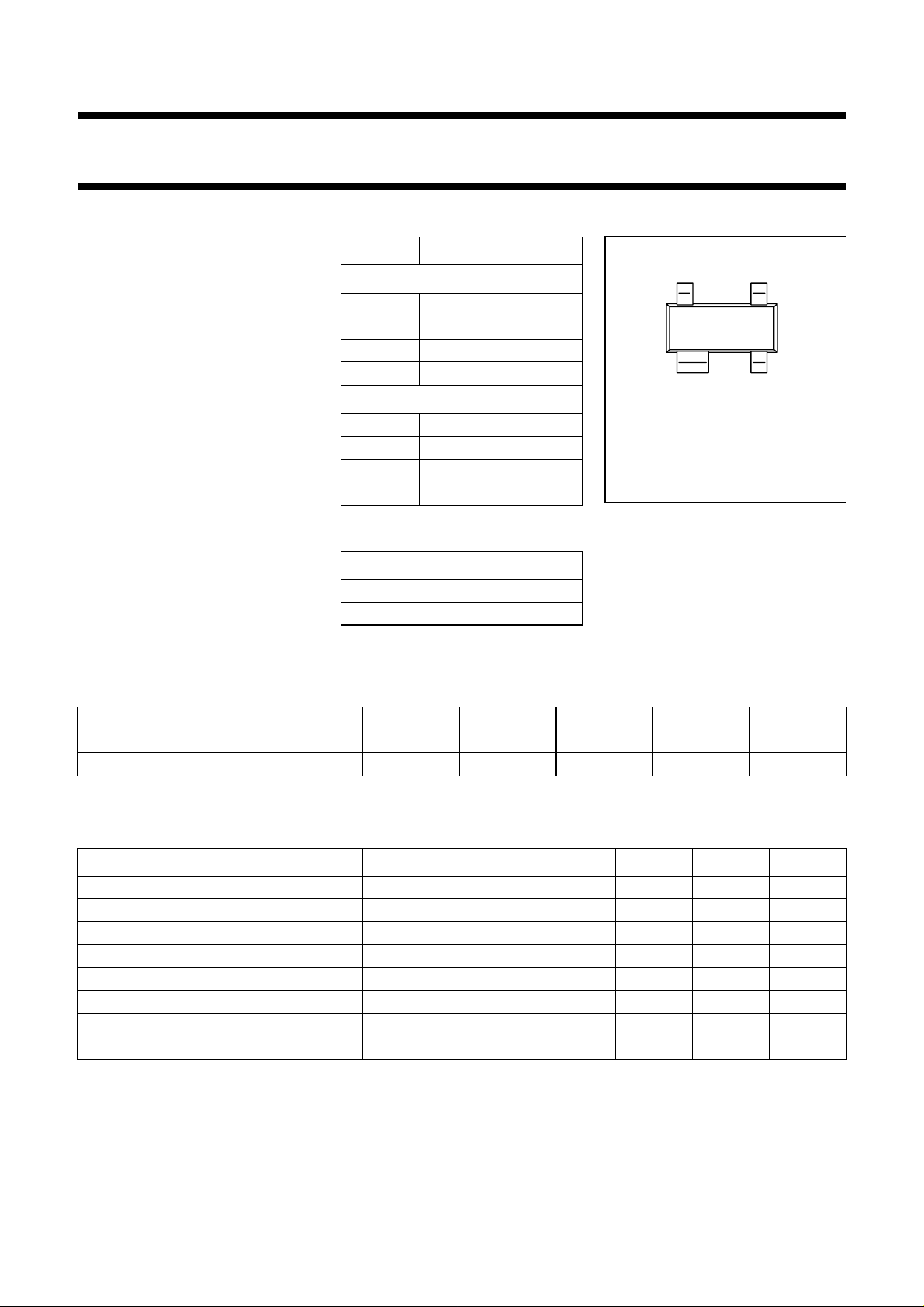
handbook, 2 columns
12
Top view
Fig.1 SOT143.
34
MSB014
QUICK REFERENCE DATA
RF performance at T
MODE OF OPERATION
=25°C in a common-emitter test circuit (see Fig.7).
amb
f
(GHz)
V
(V)
CE
P
L
(mW)
G
(dB)
p
η
(%)
Pulsed, class-AB, duty cycle: < 1 : 8 1.9 3.6 200 ≥5 ≥50
LIMITING VALUES
In accordance with the Absolute Maximum Rating System (IEC 134).
SYMBOL PARAMETER CONDITIONS MIN. MAX. UNIT
V
CBO
V
CEO
V
EBO
I
C
I
C(AV)
P
tot
T
stg
T
j
collector-base voltage open emitter − 20 V
collector-emitter voltage open base − 8V
emitter-base voltage open collector − 2.5 V
collector current (DC) − 250 mA
average collector current − 250 mA
total power dissipation up to Ts=60°C; see Fig.2; note 1 − 400 mW
storage temperature −65 +150 °C
junction temperature − 175 °C
Note
is the temperature at the soldering point of the collector pin.
1. T
s
c
1995 Aug 31 2
Page 3
Philips Semiconductors Product specification
NPN 2 GHz RF power transistor BFG10; BFG10/X
THERMAL CHARACTERISTICS
SYMBOL PARAMETER CONDITIONS VALUE UNIT
R
th j-s
thermal resistance from junction to
soldering point
Note
is the temperature at the soldering point of the collector pin.
1. T
s
CHARACTERISTICS
=25°C unless otherwise specified.
T
j
SYMBOL PARAMETER CONDITIONS MIN. MAX. UNIT
V
(BR)CBO
V
(BR)CEO
V
(BR)EBO
I
CES
h
FE
C
c
C
re
collector-base breakdown voltage open emitter; IC= 0.1 mA 20 − V
collector-emitter breakdown voltage open base; IC= 5 mA 8 − V
emitter-base breakdown voltage open collector; IE= 0.1 mA 2.5 − V
collector leakage current VCE=5V; VBE=0 − 100 µA
DC current gain IC= 50 mA; VCE=5V 25 −
collector capacitance IE=ie= 0; VCB= 3.6 V; f = 1 MHz − 3pF
feedback capacitance IC= 0; VCE= 3.6 V; f = 1 MHz − 2pF
up to Ts=60°C; note 1;
P
= 400 mW
tot
290 K/W
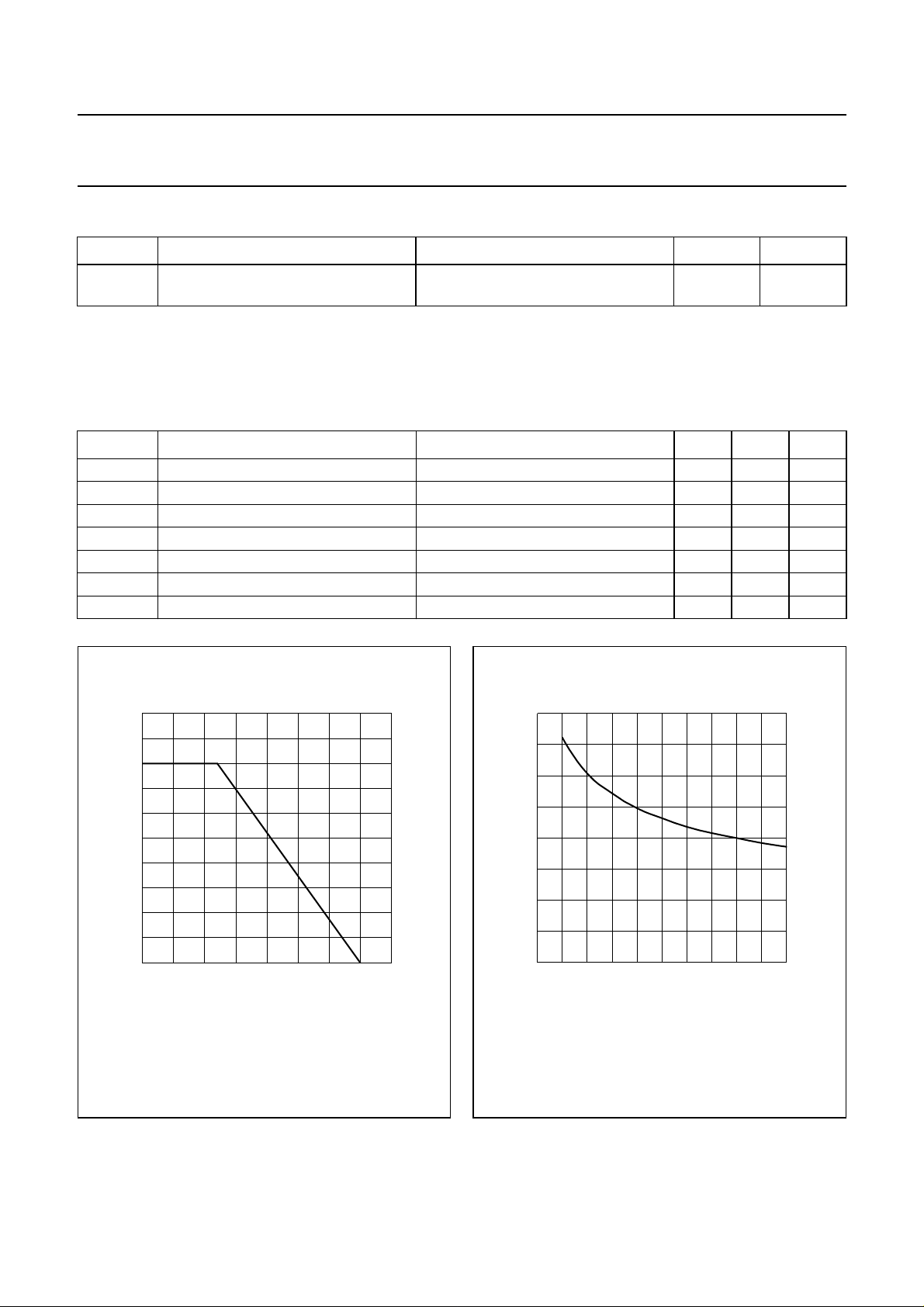
500
handbook, halfpage
P
tot
(mW)
400
300
200
100
0
0 50 100 200
150
Fig.2 Power derating curve
MLC818
o
T ( C)
s
2.0
handbook, halfpage
C
c
(pF)
1.5
1.0
0.5
0
01048
IC= 0; f= 1 MHz.
2
6
Fig.3 Collector capacitance as a function of
collector-base voltage; typical values.
MLC819
VCB(V)
1995 Aug 31 3
Page 4

Philips Semiconductors Product specification
NPN 2 GHz RF power transistor BFG10; BFG10/X
APPLICATION INFORMATION
RF performance at T
=25°C in a common-emitter test circuit (see Fig.7).
amb
MODE OF OPERATION
f
(GHz)
Pulsed, class-AB, duty cycle: < 1 : 8 1.9 3.6 1 200
V
(V)
CE
I
CQ
(mA)
P
L
(mW)
G
(dB)
p
η
(%)
c
>5 >50
typ. 7 typ. 60
Ruggedness in class-AB operation
The BFG10 is capable of withstanding a load mismatch corresponding to VSWR = 8 : 1 through all phases, at rated
output power under pulsed conditions up to a supply voltage of 7 V, f = 1.9 GHz and a duty cycle of 1 : 8.
10
handbook, halfpage
G
p
(dB)
8
6
4
2
MLC820
100
η
η
c
G
p
c
(%)
80
60
40
20
500
handbook, halfpage
P
L
(mW)
400
300
200
100
MLC821
0
Pulsed, class-AB operation.
VCE= 3.6 V; VBE= 0.65 V; f = 1.9 GHz; duty cycle < 1 : 8.
Circuit optimized for PL= 200 mW.
100 200 300 400
0 500
P (mW)
L
Fig.4 Power gain and efficiency as functions
of load power; typical values.
0
0
0 50 100 150
Pulsed, class-AB operation.
VCE= 3.6 V; VBE= 0.65 V; f = 1.9 GHz; duty cycle < 1 : 8.
Circuit optimized for PL= 200 mW.
P (mW)
D
Fig.5 Load power as a function of drive
power; typical values.
1995 Aug 31 4
Page 5

Philips Semiconductors Product specification
NPN 2 GHz RF power transistor BFG10; BFG10/X
SPICE parameters for the BFG10 crystal
SEQUENCE No. PARAMETER VALUE UNIT
1 IS 2.714 fA
2 BF 102.8 −
3 NF 0.998 −
4 VAF 28.12 V
5 IKF 6.009 A
6 ISE 403.2 pA
7 NE 2.937 −
8 BR 31.01 −
9 NR 0.999 −
10 VAR 2.889 V
11 IKR 0.284 A
12 ISC 1.487 fA
13 NC 1.100 −
14 RB 3.500 Ω
15 IRB 1.000 µA
16 RBM 3.500 Ω
17 RE 0.217 Ω
18 RC 0.196 Ω
(1)
19
20
21
(1)
(1)
XTB 0.000 −
EG 1.110 eV
XTI 3.000 −
22 CJE 5.125 pF
23 VJE 0.600 V
24 MJE 0.367 −
25 TF 12.07 ps
26 XTF 99.40 −
27 VTF 7.220 V
28 ITF 3.950 A
29 PTF 0.000 deg
30 CJC 2.327 pF
31 VJC 0.668 V
32 MJC 0.398 −
33 XCJC 0.160 −
(1)
34
35
36
37
(1)
(1)
(1)
TR 0.000 ns
CJS 0.000 F
VJS 750.0 mV
MJS 0.000 −
38 FC 0.652 −
handbook, halfpage
L1 L2
B
C
QLB= 50; QLE= 50; QL
= scaling frequency = 100 MHz.
f
c
L
be ce
Fig.6 Package equivalent circuit SOT143.
List of components (see Fig.6)
DESIGNATION VALUE UNIT
C
be
C
cb
C
ce
L1 0.12 nH
L2 0.21 nH
L3 0.06 nH
L
B
L
E
C
cb
B
E'
L
L3
E
(f)=QL
B,E
B,E
√(f/fc);
84 fF
17 fF
191 fF
0.95 nH
0.40 nH
CB' C'
C
E
MBC964
Note
1. These parameters have not been extracted,
the default values are shown.
1995 Aug 31 5
Page 6

Philips Semiconductors Product specification
NPN 2 GHz RF power transistor BFG10; BFG10/X
Test circuit information
handbook, full pagewidth
50 Ω
input
R2
C1
R1 T1
L10
L9
L1
L8
L2
C2, C3,
C4, C5
C14, C15,
C16
C11
C10
DUT
V
S
C12 C13
L7
L6
L4
L3 L5
C6, C7,
C8
C9
MLC822
50 Ω
output
V
bias
Fig.7 Common-emitter test circuit for class-AB operation at 1.9 GHz.
1995 Aug 31 6
Page 7

Philips Semiconductors Product specification
NPN 2 GHz RF power transistor BFG10; BFG10/X
List of components used in test circuit (see Fig.7)
COMPONENT DESCRIPTION VALUE DIMENSIONS CATALOGUE No.
C1, C9, C10, C11 multilayer ceramic chip capacitor; note 1 24 pF
C2, C3, C4, C5,
C6, C7
C8 multilayer ceramic chip capacitor; note 1 1.1 pF
C12, C13 electrolytic capacitor 470 µF; 10 V 2222 031 34471
C14, C15, C16 multilayer ceramic chip capacitor; note 1 10 nF
L1 stripline; note 2 length 28.5 mm
L2 stripline; note 2 length 2.3 mm
L3 stripline; note 2 length 3.1 mm
L4 stripline; note 2 length 3.3 mm
L5 stripline; note 2 length 16.3 mm
L6 stripline; note 2 length 10 mm
L7 stripline; note 2 length 4.4 mm
L8 stripline; note 2 length 19.3 mm
L9 stripline; note 2 length 19.7 mm
L10 micro choke
T1 BD228
R1 metal film resistor 20 Ω; 0.4 W 2322 157 10209
R2 metal film resistor 530 Ω; 0.4 W 2322 157 15301
multilayer ceramic chip capacitor; note 1 0.86 pF
width 0.93 mm
width 0.93 mm
width 0.93 mm
width 0.93 mm
width 0.93 mm
width 0.93 mm
width 0.4 mm
width 0.93 mm
width 0.4 mm
Notes
1. American Technical Ceramics (ATC) capacitor, type 100A or other capacitor of the same quality.
1
2. The striplines are on a
1995 Aug 31 7
⁄32inch double copper-clad printed-circuit board with PTFE fibre-glass dielectric (εr= 6).
Page 8

Philips Semiconductors Product specification
NPN 2 GHz RF power transistor BFG10; BFG10/X
handbook, full pagewidth
60
C6
C7 C8
Collector
C15
C16
Collector
L5
C12
C13
C9
MLC823
V
S
Base
V
bias
C1
T1
R2
L10
R1
L9
L1
C11
C2
Base
70
C14
L8
C3
L2 L3
C4
L7
C5
C10
L6
L4
Dimensions in mm.
The components are situated on one side of the copper-clad PTFE microfibre-glass board, the other side is not etched and
serves as a ground plane. Earth connections from the component side to the ground plane are made by through metallization.
Fig.8 Printed-circuit board and component lay-out for common-emitter test circuit in Fig.7.
1995 Aug 31 8
Page 9

Philips Semiconductors Product specification
NPN 2 GHz RF power transistor BFG10; BFG10/X
PACKAGE OUTLINE
handbook, full pagewidth
Dimensions in mm.
10
max
3.0
0.150
30
max
0.090
0.1
max
max
o
o
10
0.88
0.75
0.60
o
1.1
max
2.8
1.9
43
1
2
0
0.1
TOP VIEW
0.48
1.7
0
0.1
B
A
1.4
1.2
M0.1 AB
2.5
max
0.2
MBC845
M
AB
Fig.9 SOT143.
1995 Aug 31 9
Page 10

Philips Semiconductors Product specification
NPN 2 GHz RF power transistor BFG10; BFG10/X
DEFINITIONS
Data Sheet Status
Objective specification This data sheet contains target or goal specifications for product development.
Preliminary specification This data sheet contains preliminary data; supplementary data may be published later.
Product specification This data sheet contains final product specifications.
Limiting values
Limiting values given are in accordance with the Absolute Maximum Rating System (IEC 134). Stress above one or
more of the limiting values may cause permanent damage to the device. These are stress ratings only and operation
of the device at these or at any other conditions above those given in the Characteristics sections of the specification
is not implied. Exposure to limiting values for extended periods may affect device reliability.
Application information
Where application information is given, it is advisory and does not form part of the specification.
LIFE SUPPORT APPLICATIONS
These products are not designed for use in life support appliances, devices, or systems where malfunction of these
products can reasonably be expected to result in personal injury. Philips customers using or selling these products for
use in such applications do so at their own risk and agree to fully indemnify Philips for any damages resulting from such
improper use or sale.
1995 Aug 31 10
 Loading...