

Page 1
DISCRETE SEMICONDUCTORS
DATA SH EET
BFE505
NPN wideband differential
transistor
Product specification
Supersedes data of 1995 Sep 04
File under Discrete Semiconductors, SC14
1996 Oct 08
Page 2
Philips Semiconductors Product specification
NPN wideband differential transistor BFE505
FEATURES
• Small size
• High power gain at low bias current and voltage
• Temperature matched
• Balanced configuration
• hFE matched
• Continues to operate at VCE<1V.
APPLICATIONS
• Single balanced mixers
• Balanced amplifiers
• Balanced oscillators.
DESCRIPTION
Emitter coupled dual NPN silicon RF transistor in a surface
mount, 5-pin SOT353 (S-mini) package. The transistor is
primarily intended for applications in the RF front end as a
balanced mixer, a differential amplifier in analog and digital
cellular phones, and in cordless phones, pagers and
satellite TV-tuners.
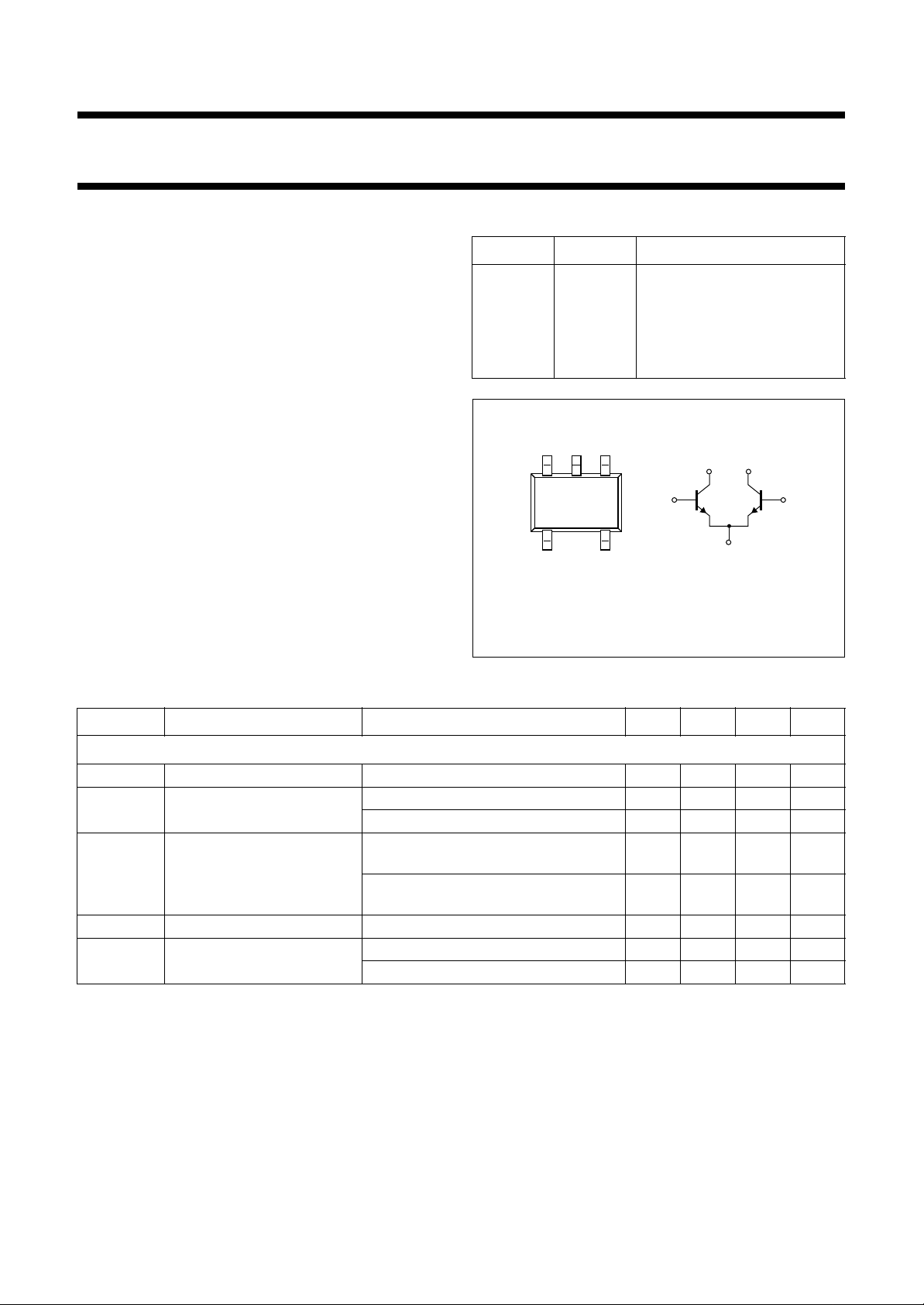
PINNING - SOT353B
SYMBOL PIN DESCRIPTION
b
1
1 base 1
e 2 emitter
b
2
c
2
c
1
handbook, halfpage
4
Top view
3 base 2
4 collector 2
5 collector 1
13
2
b
5
c
c
1
2
1
e
Fig.1 Simplified outline and symbol.
MAM211
b
2
QUICK REFERENCE DATA
SYMBOL PARAMETER CONDITIONS MIN. TYP. MAX. UNIT
Any single transistor
C
re
MSG/G
F noise figure I
h
FE
R
th j-s
feedback capacitance C
maximum power gain IC= 5 mA; VCE= 3 V; f = 900 MHz − 17 − dB
max
BCIe
= 0; VCB= 3 V; f = 1 MHz − 0.25 0.3 pF
= 5 mA; VCE= 3 V; f = 2 GHz − 10 − dB
I
C
= 2 mA; VCE= 3 V; f = 900 MHz;
C
ΓS= Γ
opt
= 3 mA; VCE= 3 V; f = 2 GHz;
I
C
ΓS= Γ
opt
− 1.2 1.7 dB
− 1.9 2.1 dB
DC current gain IC= 5 mA; VCE= 3 V 60 120 250
thermal resistance from
junction to soldering point
single loaded −−230 K/W
double loaded −−115 K/W
1996 Oct 08 2
Page 3
Philips Semiconductors Product specification
NPN wideband differential transistor BFE505
LIMITING VALUES
In accordance with the Absolute Maximum System (IEC 134).
SYMBOL PARAMETER CONDITIONS MIN. MAX. UNIT
Any single transistor
V
CBO
V
CEO
V
EBO
I
C
P
tot
T
stg
T
j
THERMAL CHARACTERISTICS
SYMBOL PARAMETER CONDITIONS VALUE UNIT
R
th j-s
collector-base voltage open emitter − 20 V
collector-emitter voltage open base − 8V
emitter-base voltage open collector − 2.5 V
DC collector current − 18 mA
total power dissipation up to Ts=118°C; note 1 − 500 mW
storage temperature −65 +175 °C
operating junction temperature − 175 °C
thermal resistance from junction
to soldering point; note 1
single loaded 230 K/W
double loaded 115 K/W
Note to the Limiting values and Thermal characteristics
1. T
is the temperature at the soldering point of the collector pin.
s
1996 Oct 08 3
Page 4

Philips Semiconductors Product specification
NPN wideband differential transistor BFE505
CHARACTERISTICS
T
=25°C unless otherwise specified.
j
SYMBOL PARAMETER CONDITIONS MIN. TYP. MAX. UNIT
DC characteristics of any single transistor
V
(BR)CBO
V
(BR)CEO
V
(BR)EBO
I
CBO
h
FE
DC characteristics of the dual transistor
∆h
FE
∆V
BEO
collector-base breakdown voltage IC= 2.5 µA; IE=0 20 −−V
collector-emitter breakdown voltage IC=10µA; IB=0 8 −−V
emitter-base breakdown voltage IE= 2.5 µA; IC= 0 2.5 −−V
collector-base leakage current IE= 0; VCB=6V −−50 nA
DC current gain IC= 5 mA; VCE= 6 V 60 120 250
ratio of highest and lowest DC
current gain
difference between highest and
IC1=IC2= 5 mA;
V
CE1=VCE2
=6V
IE1=IE2= 10 mA; T
1 1.2 −
=25°C0 1 − mV
amb
lowest base-emitter voltage
(offset voltage)
AC characteristics of any single transistor
f
T
C
c
C
re
MSG/G
2
s
21
F noise figure I
transition frequency IC= 5 mA; VCE= 3 V; f = 1 GHz − 9 − GHz
collector capacitance IE=ie= 0; VCB= 3 V; f = 1 MHz − 0.3 − pF
feedback capacitance IC= 0; VCB=3V;f=1MHz − 0.25 − pF
maximum power gain; note 1 IC= 5 mA; VCE=3V;
max
f = 900 MHz; T
= 5 mA; VCE=3V;
I
C
f = 2 GHz; T
insertion power gain I
= 5 mA; VCE=3V;
C
f = 900 MHz; T
= 2 mA; VCE=3V;
C
f = 900 MHz; ΓS= Γ
= 3 mA; VCE=3V;
I
C
f = 2 GHz; ΓS= Γ
amb
=25°C
amb
=25°C
=25°C
amb
opt
opt
− 17 − dB
− 10 − dB
− 13 − dB
− 1.2 1.7 dB
− 1.9 2.1 dB
Note
1. Maximum gain of the differential amplifier is higher because of internal emitter connection (see Fig.2).
1996 Oct 08 4
Page 5

Philips Semiconductors Product specification
NPN wideband differential transistor BFE505
APPLICATION INFORMATION
SPICE parameters for any single BFE505 die
SEQUENCE No. PARAMETER VALUE UNIT
1 IS 134.1 aA
2 BF 180.0 −
3 NF 0.988 −
4 VAF 38.34 V
5 IKF 150.0 mA
6 ISE 27.81 fA
7 NE 2.051 −
8 BR 55.19 −
9 NR 0.982 −
10 VAR 2.459 V
11 IKR 2.920 mA
12 ISC 17.45 aA
13 NC 1.062 −
14 RB 20.00 Ω
15 IRB 1.000 µA
16 RBM 20.00 Ω
17 RE 1.171 Ω
18 RC 4.350 Ω
(1)
19
20
21
(1)
(1)
XTB 0.000 −
EG 1.110 eV
XTI 3.000 −
22 CJE 284.7 fF
23 VJE 600.0 mV
24 MJE 0.303 −
25 TF 7.037 ps
26 XTF 12.34 −
27 VTF 1.701 V
28 ITF 30.64 mA
29 PTF 0.000 deg
30 CJC 242.4 fF
31 VJC 188.6 mV
32 MJC 0.041 −
33 XCJC 0.130 −
34 TR 1.332 ns
(1)
35
36
37
(1)
(1)
CJS 0.000 F
VJS 750.0 mV
MJS 0.000 −
38 FC 0.897 −
handbook, halfpage
B1 B2
LB LB
C1 C2
LP LP
T1 T2
LE
LP
E
LE
Fig.2 Package equivalent circuit SOT353B
(inductance only).
Lead inductances (nH)
35
0.4
0.8
0.6
LP
LB
LE
35E
B2
3.5 35
C2
2
C1
36 35 23615
B1 E B2 C2
Fig.3 Package capacitance (fF) between
indicated nodes.
MBG190
MBG191
Note
1. These parameters have not been extracted, the
default values are shown.
1996 Oct 08 5
Page 6

Philips Semiconductors Product specification
NPN wideband differential transistor BFE505
Typical application circuit
handbook, full pagewidth
Fig.4 Single balanced switching mixer amplifier, featuring high LO↔RF isolation and linearity.
LO in
+V
CC
+V
MBG192
IF out
RF in
CC
1996 Oct 08 6
Page 7

Philips Semiconductors Product specification
NPN wideband differential transistor BFE505
PACKAGE OUTLINE
handbook, full pagewidth
Dimensions in mm.
1.0
0.8
0.2
0.8
0.6
0.65
0.65
MSA365
0.1
0.0
A
1
2
3
0.3
0.1
1.35
1.15
2.2
2.0
Fig.5 SOT353.
0.17
0.10
0.2
M
B
B
5
0.25
2.2
0.15
1.8
(5x)
4
0.2
AM
1996 Oct 08 7
Page 8

Philips Semiconductors Product specification
NPN wideband differential transistor BFE505
DEFINITIONS
Data sheet status
Objective specification This data sheet contains target or goal specifications for product development.
Preliminary specification This data sheet contains preliminary data; supplementary data may be published later.
Product specification This data sheet contains final product specifications.
Short-form specification The data in this specification is extracted from a full data sheet with the same type
number and title. For detailed information see the relevant data sheet or data handbook.
Limiting values
Limiting values given are in accordance with the Absolute Maximum Rating System (IEC 134). Stress above one or
more of the limiting values may cause permanent damage to the device. These are stress ratings only and operation
of the device at these or at any other conditions above those given in the Characteristics sections of the specification
is not implied. Exposure to limiting values for extended periods may affect device reliability.
Application information
Where application information is given, it is advisory and does not form part of the specification.
LIFE SUPPORT APPLICATIONS
These products are not designed for use in life support appliances, devices, or systems where malfunction of these
products can reasonably be expected to result in personal injury. Philips customers using or selling these products for
use in such applications do so at their own risk and agree to fully indemnify Philips for any damages resulting from such
improper use or sale.
1996 Oct 08 8
 Loading...