

Page 1

DISCRETE SEMICONDUCTORS
DATA SH EET
BFC505
NPN wideband cascode transistor
Product specification
Supersedes data of 1995 Sep 01
File under Discrete Semiconductors, SC14
1996 Oct 08
Page 2
Philips Semiconductors Product specification
NPN wideband cascode transistor BFC505
FEATURES
• Small size
• High power gain at low bias current and high
frequencies
• High reverse isolation
• Low noise figure
• Gold metallization ensures excellent reliability
• Minimum operating voltage V
C2−E1
=1V.
APPLICATIONS
• Low voltage, low current, low noise and high gain
amplifiers
• Oscillator buffer amplifiers
• Wideband voltage-to-current converters.
DESCRIPTION
Cascode amplifier with two discrete dies in a surface
mount, 5-pin SOT353 (S-mini) package. The amplifier is
primarily intended for low power RF communications
equipment, such as pagers and has a very low feedback
capacitance resulting in high isolation.
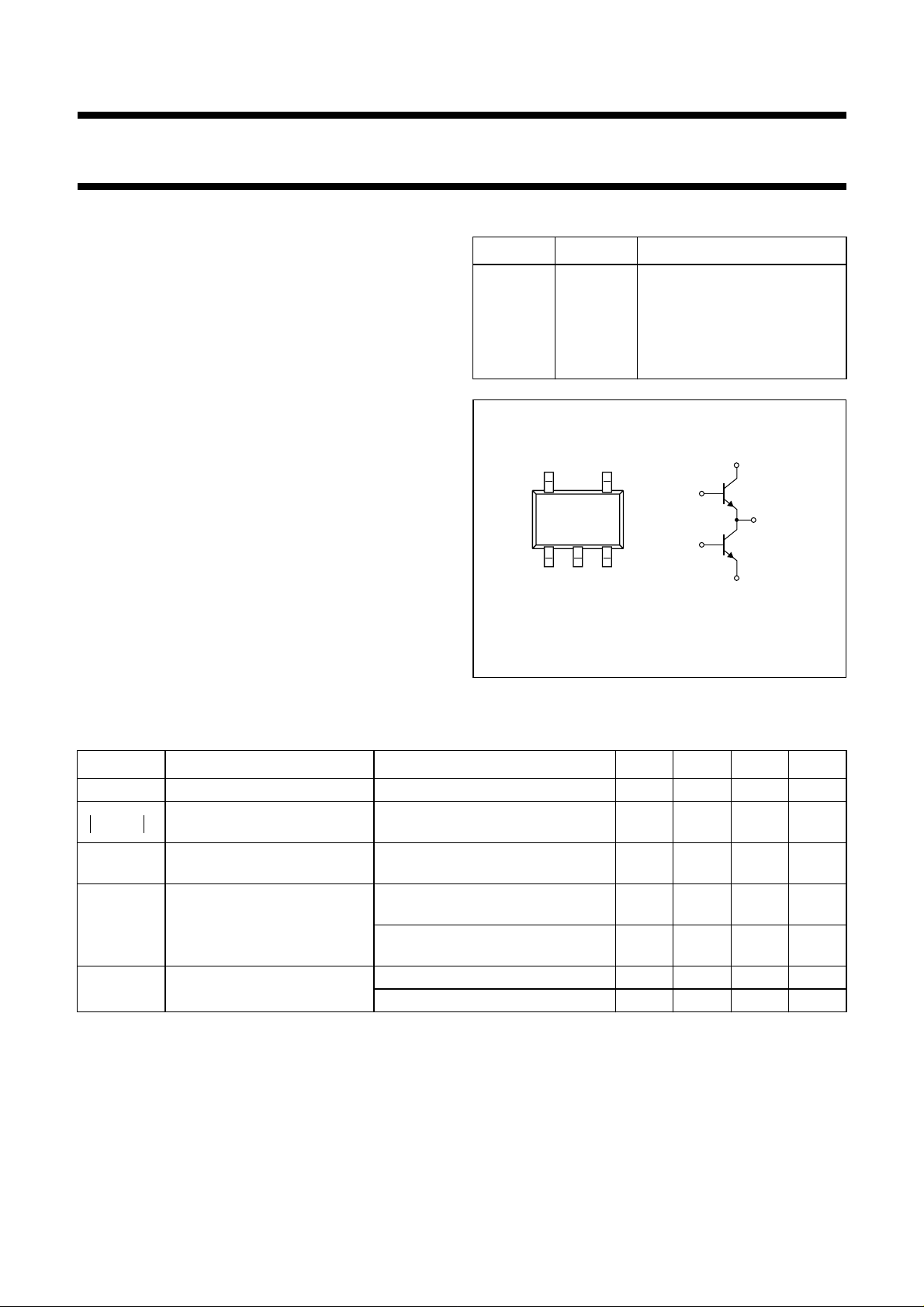
PINNING - SOT353
PIN SYMBOL DESCRIPTION
1b
2e
3b
4c
1
5c
handbook, halfpage
5
2
Top view
/e
base 2
2
emitter 1
1
base 1
1
collector 1/emitter 2
2
collector 2
2
4
31
b
2
b
1
Fig.1 Simplified outline and symbol.
c
e
2
1
c1/e
MAM212
2
QUICK REFERENCE DATA
b
connected to ground via 1 nF (0603) capacitor, e1 connected directly to ground.
2
SYMBOL PARAMETER CONDITIONS MIN. TYP. MAX. UNIT
C
re
s21s12⁄
feedback capacitance C
maximum isolation I
2
B1−C2Ie
MSG maximum stable power gain I
F noise figure I
R
th j-s
thermal resistance from
junction to soldering point
= 0; V
= 5 mA; VC2=VB2=3V;
C
= 0; f = 1 MHz −−10 fF
C2-E1
60 −−dB
f = 900 MHz
= 0.5 mA; VC2=VB2=1V;
C
f = 900 MHz; T
= 0.5 mA; V
C
f = 500 MHz; ΓS= Γ
= 1 mA; V
I
C
f = 900 MHz; ΓS= Γ
amb
C2-E1
C2-E1
=25°C
=1V;
opt
=3V;
opt
− 22 − dB
− 1.1 1.4 dB
− 1.8 2.1 dB
single loaded −−230 K/W
double loaded −−115 K/W
1996 Oct 08 2
Page 3
Philips Semiconductors Product specification
NPN wideband cascode transistor BFC505
LIMITING VALUES
In accordance with the Absolute Maximum System (IEC 134).
SYMBOL PARAMETER CONDITIONS MIN. MAX. UNIT
Any single transistor
V
CBO
V
CEO
V
EBO
I
C
P
tot
T
stg
T
j
THERMAL CHARACTERISTICS
SYMBOL PARAMETER CONDITIONS VALUE UNIT
R
th j-s
collector-base voltage open emitter − 20 V
collector-emitter voltage open base − 8V
emitter-base voltage open collector − 2.5 V
DC collector current − 18 mA
total power dissipation up to Ts=118°C; note 1 − 500 mW
storage temperature −65 +175 °C
junction temperature − 175 °C
thermal resistance from junction
to soldering point; note 1
single loaded 230 K/W
double loaded 115 K/W
Note to the Limiting values and Thermal characteristics
1. T
is the temperature at the soldering point of the collector pin.
s
1996 Oct 08 3
Page 4
Philips Semiconductors Product specification
NPN wideband cascode transistor BFC505
CHARACTERISTICS
T
=25°C unless otherwise specified.
j
SYMBOL PARAMETER CONDITIONS MIN. TYP. MAX. UNIT
DC characteristics of any single transistor
V
(BR)CBO
V
(BR)CEO
V
(BR)EBO
I
CBO
h
FE
AC characteristics of the cascode configuration measured in test circuit (note 1)
f
T
C
c
C
re2
C
re
MSG maximum stable power gain;
2
s
21
s21s12⁄
F noise figure I
IP
3
collector-base breakdown voltage IC= 2.5 µA; IE=0 20 −−V
collector-emitter breakdown
IC=10µA; IB=0 8 −−V
voltage
emitter-base breakdown voltage IE= 2.5 µA; IC= 0 2.5 −−V
collector-base leakage current IE= 0; VCB=6V −−50 nA
DC current gain IC= 5 mA; VCE= 6 V 60 120 250
transition frequency IC= 5 mA; V
collector capacitance T2 IE=ie= 0; V
feedback capacitance T2 IC= 0; V
feedback capacitance IC= 0; V
I
= 0.25 mA; V
C
note 2
f = 300 MHz; T
I
= 0.5 mA; V
C
f = 900 MHz; T
I
= 5 mA; V
C
T
amb
insertion power gain I
= 0.5 mA; V
C
f = 300 MHz; T
I
= 5 mA; V
C
f = 900 MHz; T
I
= 5 mA; V
C
T
amb
maximum isolation; note 3 I
2
= 0.5 mA; V
C
C2-E1
C2-E1
=25°C
=25°C
= 3 V; f = 1 GHz − 7.3 − GHz
C2-E1
= 0; f = 1 MHz − 0.4 − pF
C2-B2
=3V;f=1MHz − 250 fF
=3V;f=1MHz −−10 fF
=1V;
C2-E1
=25°C
amb
=1V;
C2-E1
=25°C
amb
= 3 V; f = 2 GHz;
C2-E1
=3V;
C2-E1
=25°C
amb
=3V;
C2-E1
=25°C
amb
= 3 V; f = 2 GHz;
C2-E1
=1V;
C2-E1
− 25 − dB
− 22 − dB
− 23 − dB
− 21 − dB
− 16 − dB
− 11 − dB
40 45 − dB
f = 900 MHz
I
= 5 mA; V
C
C2-E1
=3V;
60 68 − dB
f = 900 MHz
= 5 mA; V
I
C
= 0.5 mA; V
C
f = 500 MHz; ΓS= Γ
I
= 1 mA; V
C
f = 900 MHz; ΓS= Γ
= 1 mA; V
I
C
f = 2 GHz; ΓS= Γ
= 3 V; f = 2 GHz 40 48 − dB
C2-E1
C2-E1
C2-E1
C2-E1
=1V;
opt
=3V;
opt
=1V;
opt
− 1.1 1.4 dB
− 1.8 2.1 dB
− 3.5 − dB
third order intercept point (input) note 4 −−20 − dBm
1996 Oct 08 4
Page 5

Philips Semiconductors Product specification
NPN wideband cascode transistor BFC505
Notes
1. VB2=V
2. MSG = ;
3. Maximum isolation is defined as the isolation when S21 of the amplifier is reduced to unity (buffer application).
4. IC= 1 mA; VCE= 3 V; RS=50Ω; ZL= opt; T
f
(2p−q)
/2 + 0.6 V
C2−E1
s12s21⁄ kk21––
× k
= 904 MHz.
1s
=
-----------------------------------------------------------------------------------------------------------------
× s12s21×–
11s22
2s
=25°C; fp= 900 MHz; fq= 902 MHz; measured at
amb
2
–+
s21××
12
2
s
–
11
2
s
22
150
Ts (
MBG208
o
C)
600
handbook, halfpage
P
tot
(mW)
400
200
0
0 50 100 200
double loaded
single loaded
Fig.2 Power derating as a function of soldering
point temperature; typical values.
12
handbook, halfpage
f
T
(GHz)
8
4
0
10
f =1 GHz; T
−1
amb
=25°C.
V
C2-E1 = 12 V
9 V
6 V
3 V
110
IC (mA)
Fig.3 Transition frequency as a function of
collector current; typical values.
MBG209
2
10
1996 Oct 08 5
Page 6

Philips Semiconductors Product specification
NPN wideband cascode transistor BFC505
handbook, halfpage
6
F
IC = 0.25 mA
(dB)
4
1 mA
2
0
−1
V
C2-E1
10
=1V.
1
f (GHz)
Fig.4 Minimum noise figure as a function of
frequency; typical values.
MGG213
MGG214
10
V
(dB)
C2-E1
F
6
4
2
0
−1
10
=1V.
f = 900 MHz
500 MHz
1
IC (mA)
handbook, halfpage
10
Fig.5 Minimum noise figure as a function of
collector current; typical values.
50
andbook, halfpage
MSG
(dB)
40
(1)
(2)
(3)
30
20
10
10 10
(1) IC= 5 mA; V
(2) IC= 1 mA; V
(3) IC= 0.5 mA; V
C2−E1
C2−E1
C2−E1
2
=3V.
=1V.
=1V.
3
10
f (MHz)
Fig.6 Maximum stable gain and isolation as
functions of frequency; typical values.
MGG215
MGG216
100
S21/S
80
60
(dB)
40
andbook, halfpage
12
MSG
(dB)
(1)
30
(2)
(3)
20
80
S21/S
(dB)
60
40
12
40
20
4
10
(1) V
(2) V
(3) V
10
−1
10
= 1 V; f = 500 MHz.
C2−E1
= 1 V; f = 900 MHz.
C2−E1
= 3 V; f = 2 GHz.
C2−E1
1
IC (mA)
20
10
Fig.7 Maximum stable gain and isolation as
functions of collector current; typical values.
1996 Oct 08 6
Page 7

Philips Semiconductors Product specification
NPN wideband cascode transistor BFC505
25
handbook, halfpage
gain
(dB)
20
15
10
5
0
−5
−1
10
VCE= 1 V; RS=50Ω; XS=XL= opt; f = 900MHz.
RL = 470 Ω
50 Ω
1
IC (mA)
MGG217
Fig.8 Transducer gain as a function of collector
current; typical values.
10
handbook, halfpage
IP
3
(dBm)
0
−10
−20
−30
10
Point tuned for maximum gain with double slug tuners; f = 900 MHz.
(1) IP3(output); V
(3) IP3(input); V
−1
10
=3V. (2) IP3(output); V
C2-E1
=3V. (4) IP3(input); V
C2-E1
(1)
(2)
(3)
(4)
110
I
MGG218
(mA)
C
=1V.
C2-E1
=1V.
C2-E1
Fig.9 Third order intercept point as a function of
collector current; typical values.
1996 Oct 08 7
Page 8

Philips Semiconductors Product specification
NPN wideband cascode transistor BFC505
APPLICATION INFORMATION
SPICE parameters for any single BFC505 die
SEQUENCE No. PARAMETER VALUE UNIT
1 IS 134.1 aA
2 BF 180.0 −
3 NF 0.988 −
4 VAF 38.34 V
5 IKF 150.0 mA
6 ISE 27.81 fA
7 NE 2.051 −
8 BR 55.19 −
9 NR 0.982 −
10 VAR 2.459 V
11 IKR 2.920 mA
12 ISC 17.45 aA
13 NC 1.062 −
14 RB 20.00 Ω
15 IRB 1.000 µA
16 RBM 20.00 Ω
17 RE 1.171 Ω
18 RC 4.350 Ω
19
20
21
(1)
(1)
(1)
XTB 0.000 −
EG 1.110 eV
XTI 3.000 −
22 CJE 284.7 fF
23 VJE 600.0 mV
24 MJE 0.303 −
25 TF 7.037 ps
26 XTF 12.34 −
27 VTF 1.701 V
28 ITF 30.64 mA
29 PTF 0.000 deg
30 CJC 242.4 fF
31 VJC 188.6 mV
32 MJC 0.041 −
33 XCJC 0.130 −
34 TR 1.332 ns
(1)
35
36
37
(1)
(1)
CJS 0.000 F
VJS 750.0 mV
MJS 0.000 −
38 FC 0.897 −
handbook, halfpage
B2
B1
LP
LP LB1
LB2
LP
T2
LE2
LP
T1
LE1
Fig.10 Package equivalent circuit SOT353A
(inductance only).
Lead and mutual inductances (nH)
LP
LB1,2
LE1,2
C1/E2
0.4
0.5
0.8
35E1
B2
3.5 35
C2
2
35
36 35 23615
B1 E1 B2 C2
M(LB1,LE1)
M(LB1,LE2)
C2
C1/E2
LP
MBG217
E1
MBG216
+0.4
+0.25
Note
1. These parameters have not been extracted, the
default values are shown.
1996 Oct 08 8
Fig.11 Package capacitance (fF) between
indicated nodes.
Page 9

Philips Semiconductors Product specification
NPN wideband cascode transistor BFC505
Typical application circuits
handbook, full pagewidth
RS increases stability.
RF input
(50 Ω)
CD
RB1
CB
RB2
C2C1
C
inLin
RB3
RE
Fig.12 Narrowband amplifier.
RS
L
out
C
par
CE
MBG218
+V
CC
RP
C3
C
out
RF output
(50 Ω)
C4
handbook, full pagewidth
E1
V
tune
T1 forms a colpitts oscillator.
T2 acts as a buffer amplifier.
Fig.13 VCO/buffer combination.
1996 Oct 08 9
T2
T1
E1
MBG227
+V
CC
RF output
Page 10

Philips Semiconductors Product specification
NPN wideband cascode transistor BFC505
PACKAGE OUTLINE
handbook, full pagewidth
Dimensions in mm.
1.0
0.8
0.2
0.8
0.6
0.65
0.65
MSA365
0.1
0.0
A
1
2
3
Fig.14 SOT353.
1.35
1.15
2.2
2.0
0.3
0.1
0.17
0.10
0.2
M
B
B
5
0.25
2.2
0.15
1.8
(5x)
4
0.2
AM
1996 Oct 08 10
Page 11

Philips Semiconductors Product specification
NPN wideband cascode transistor BFC505
DEFINITIONS
Data sheet status
Objective specification This data sheet contains target or goal specifications for product development.
Preliminary specification This data sheet contains preliminary data; supplementary data may be published later.
Product specification This data sheet contains final product specifications.
Short-form specification The data in this specification is extracted from a full data sheet with the same type
number and title. For detailed information see the relevant data sheet or data handbook.
Limiting values
Limiting values given are in accordance with the Absolute Maximum Rating System (IEC 134). Stress above one or
more of the limiting values may cause permanent damage to the device. These are stress ratings only and operation
of the device at these or at any other conditions above those given in the Characteristics sections of the specification
is not implied. Exposure to limiting values for extended periods may affect device reliability.
Application information
Where application information is given, it is advisory and does not form part of the specification.
LIFE SUPPORT APPLICATIONS
These products are not designed for use in life support appliances, devices, or systems where malfunction of these
products can reasonably be expected to result in personal injury. Philips customers using or selling these products for
use in such applications do so at their own risk and agree to fully indemnify Philips for any damages resulting from such
improper use or sale.
1996 Oct 08 11
 Loading...