

Page 1
DISCRETE SEMICONDUCTORS
DATA SH EET
BF998; BF998R
Silicon N-channel dual-gate
MOS-FETs
Product specification
Supersedes data of April 1991
File under Discrete Semiconductors, SC07
1996 Aug 01
Page 2
Philips Semiconductors Product specification
Silicon N-channel dual-gate MOS-FETs BF998; BF998R
FEATURES
• Short channel transistor with high forward transfer
admittance to input capacitance ratio
• Low noise gain controlled amplifier up to 1 GHz.
APPLICATIONS
• VHF and UHF applications with 12 V supply voltage,
such as television tuners and professional
communications equipment.
DESCRIPTION
Depletion type field effect transistor in a plastic
microminiature SOT143 or SOT143R package with source
and substrate interconnected. The transistors are
protected against excessive input voltage surges by
integrated back-to-back diodes between gates and
source.
CAUTION
The device is supplied in an antistatic package. The
gate-source input must be protected against static
discharge during transport or handling.
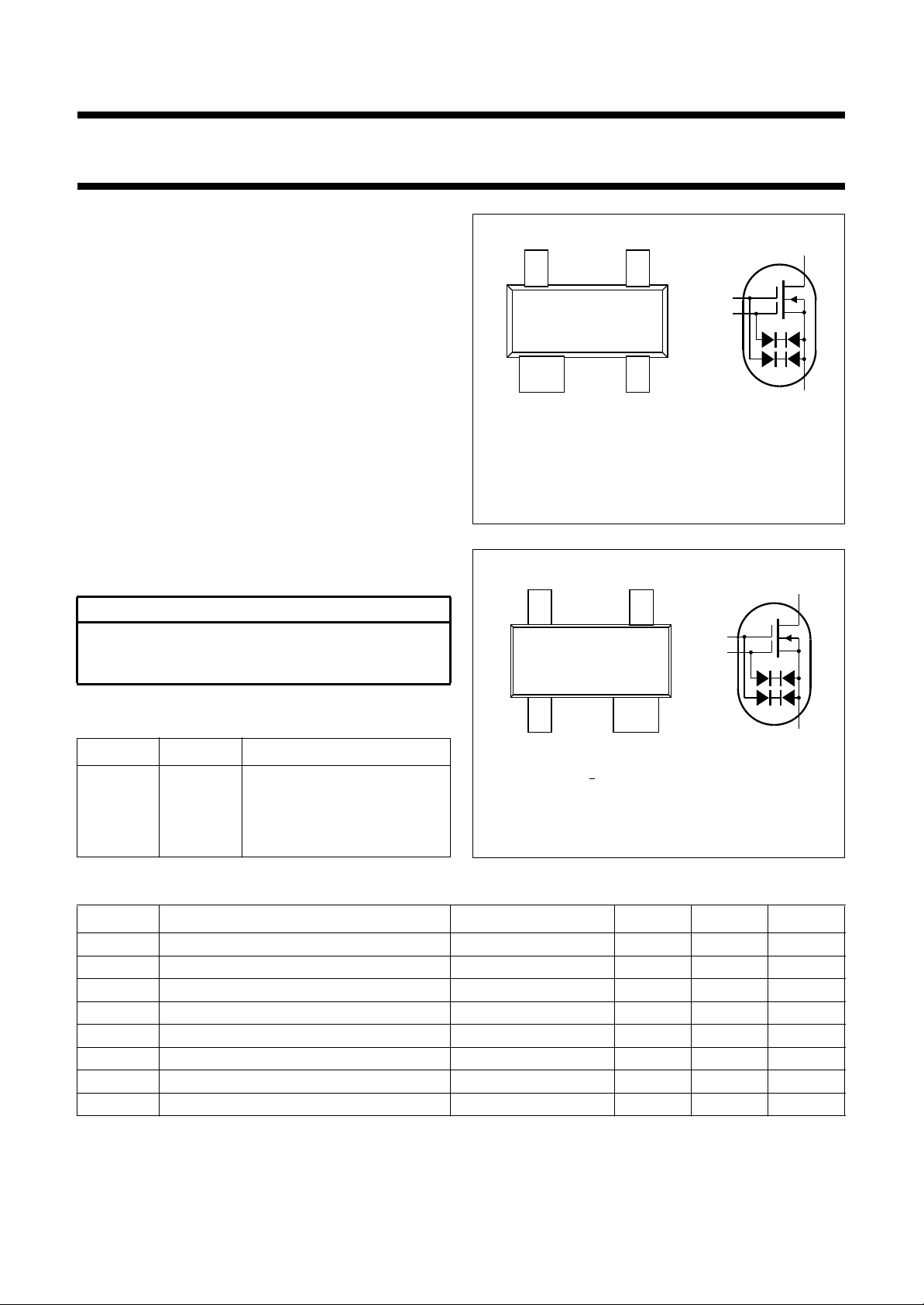
handbook, halfpage
Top view
Marking code: MOp.
Fig.1 Simplified outline (SOT143)
handbook, halfpage
43
21
and symbol; BF998.
34
MAM039
g
g
d
g
2
g
1
s,b
d
2
1
PINNING
PIN SYMBOL DESCRIPTION
1 s, b source
Top view
Marking code: MOp.
12
MAM040
2 d drain
3g
4g
gate 2
2
gate 1
1
Fig.2 Simplified outline (SOT143R)
and symbol; BF998R.
QUICK REFERENCE DATA
SYMBOL PARAMETER CONDITIONS TYP. MAX. UNIT
V
DS
I
D
P
tot
forward transfer admittance 24 − mS
y
fs
C
ig1-s
C
rs
drain-source voltage − 12 V
drain current − 30 mA
total power dissipation − 200 mW
input capacitance at gate 1 2.1 − pF
reverse transfer capacitance f = 1 MHz 25 − fF
F noise figure f = 800 MHz 1 − dB
T
j
operating junction temperature − 150 °C
s,b
1996 Aug 01 2
Page 3
Philips Semiconductors Product specification
Silicon N-channel dual-gate MOS-FETs BF998; BF998R
LIMITING VALUES
In accordance with the Absolute Maximum Rating System (IEC 134).
SYMBOL PARAMETER CONDITIONS MIN. MAX. UNIT
V
DS
I
D
±I
G1
±I
G2
P
tot
P
tot
T
stg
T
j
Notes
1. Device mounted on a ceramic substrate, 8 mm × 10 mm × 0.7 mm.
2. Device mounted on a printed-circuit board.
drain-source voltage − 12 V
drain current − 30 mA
gate 1 current − 10 mA
gate 2 current − 10 mA
total power dissipation; BF998 up to T
up to T
total power dissipation; BF998R up to T
=60°C; see Fig.3; note 1 − 200 mW
amb
=50°C; see Fig.3; note 2 − 200 mW
amb
=50°C; see Fig.4; note 1 − 200 mW
amb
storage temperature −65 +150 °C
operating junction temperature − 150 °C
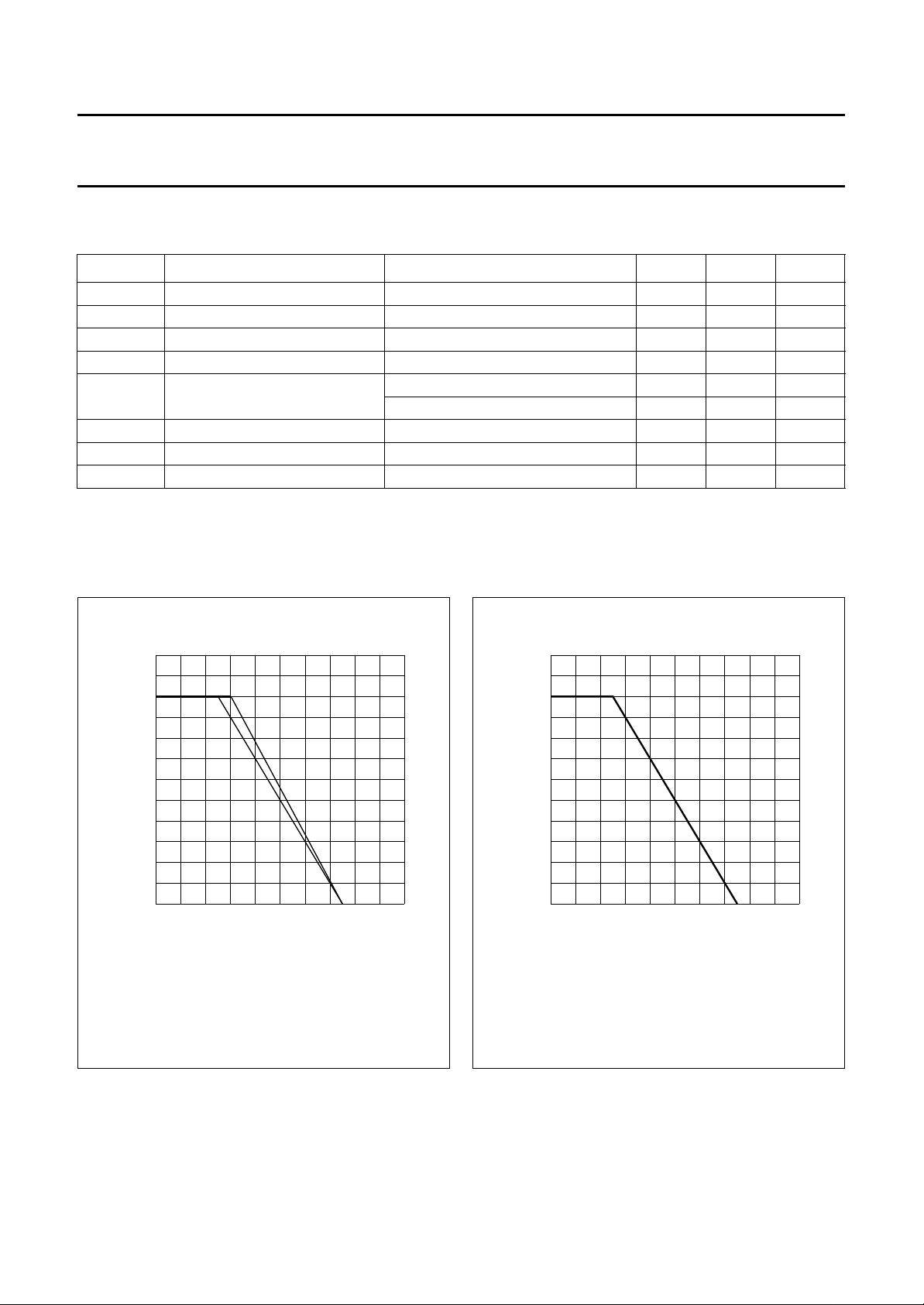
handbook, halfpage
200
P
tot max
(mW)
100
0
0 200100
(1) Ceramic substrate.
(2) Printed-circuit board.
(2) (1)
Fig.3 Power derating curves; BF998.
T
amb
o
( C)
MLA198
handbook, halfpage
200
P
tot max
(mW)
100
0
0 200100
Fig.4 Power derating curve; BF998R.
T
amb
MGA002
(°C)
1996 Aug 01 3
Page 4
Philips Semiconductors Product specification
Silicon N-channel dual-gate MOS-FETs BF998; BF998R
THERMAL CHARACTERISTICS
SYMBOL PARAMETER CONDITIONS VALUE UNIT
R
th j-a
R
th j-a
Notes
1. Device mounted on a ceramic substrate, 8 mm × 10 mm × 0.7 mm.
2. Device mounted on a printed-circuit board.
STATIC CHARACTERISTICS
=25°C; unless otherwise specified.
T
j
SYMBOL PARAMETER CONDITIONS MIN. MAX. UNIT
±V
(BR)G1-SS
±V
(BR)G2-SS
−V
(P)G1-S
−V
(P)G2-S
I
DSS
±I
G1-SS
±I
G2-SS
thermal resistance from junction to ambient in free air; BF998 note 1 460 K/W
note 2 500 K/W
thermal resistance from junction to ambient in free air; BF998R note 1 500 K/W
gate 1-source breakdown voltage V
gate 2-source breakdown voltage V
gate 1-source cut-off voltage V
gate 2-source cut-off voltage V
drain-source current V
gate 1 cut-off current V
gate 2 cut-off current V
G2-S=VDS
G1-S=VDS
G2-S
G1-S
G2-S
G2-S=VDS
G1-S=VDS
= 0; I
= 0; I
= ±10 mA 6 20 V
G1-SS
= ±10 mA 6 20 V
G2-SS
=4V; VDS=8V; ID=20µA − 2.0 V
= 0; VDS=8V; ID=20µA − 1.5 V
=4V; VDS=8V; V
= 0; V
G1-S
= 0; V
G2-S
= 0; note 1 2 18 mA
G1-S
= ±5V − 50 nA
= ±5V − 50 nA
Note
1. Measured under pulse condition.
DYNAMIC CHARACTERISTICS
Common source; T
=25°C; VDS=8V;V
amb
= 4 V; ID= 10 mA.
G2-S
SYMBOL PARAMETER CONDITIONS MIN. TYP. MAX. UNIT
y
forward transfer admittance f = 1 kHz 21 24 − mS
fs
C
ig1-s
C
ig2-s
C
os
C
rs
F noise figure f = 200 MHz; G
input capacitance at gate 1 f = 1 MHz − 2.1 2.5 pF
input capacitance at gate 2 f = 1 MHz − 1.2 − pF
output capacitance f = 1 MHz − 1.05 − pF
reverse transfer capacitance f = 1 MHz − 25 − fF
f = 800 MHz; G
= 2 mS; BS=B
S
= 3.3 mS; BS=B
S
Sopt
− 0.6 − dB
− 1.0 − dB
Sopt
1996 Aug 01 4
Page 5

Philips Semiconductors Product specification
Silicon N-channel dual-gate MOS-FETs BF998; BF998R
24
handbook, halfpage
ID
(mA)
20
16
12
8
4
0
010
V
= 4V; T
G2-S
2468
=25°C.
amb
Fig.5 Output characteristics; typical values.
VDS (V)
MGE813
V
G1-S
0.4 V
0.3 V
0.2 V
0.1 V
0 V
−0.1 V
−0.2 V
−0.3 V
−0.4 V
−0.5 V
3 V
G1
MGE815
2 V
1 V
0 V
(V)
24
handbook, halfpage
=
ID
(mA)
20
16
12
8
4
0
−11
VDS= 8 V; T
amb
=25°C.
V
G2-S
= 4 V
0
V
Fig.6 Transfer characteristics; typical values.
24
handbook, halfpage
ID
(mA)
20
16
12
8
4
0
−1600 −400−800−1200 400
VDS= 8 V; V
G2-S
= 4 V; T
amb
V
=25°C.
Fig.7 Drain current as a function of gate 1
voltage; typical values.
max
G1
0
(mV)
MGE814
typ
min
161284
ID (mA)
MGE811
0.5 V
4 V
3 V
2 V
1 V
30
handbook, halfpage
|yfs|
(mS)
24
18
12
6
0
020
VDS= 8 V; T
amb
V
G2-S
=25°C.
= 0 V
Fig.8 Forward transfer admittance as a function of
drain current; typical values.
1996 Aug 01 5
Page 6

Philips Semiconductors Product specification
Silicon N-channel dual-gate MOS-FETs BF998; BF998R
30
handbook, halfpage
|yfs|
(mS)
24
18
12
6
0
−11
VDS= 8 V; T
amb
=25°C.
0
VG1 (V)
V
G2-S
MGE812
= 4 V
3 V
2 V
1 V
0 V
Fig.9 Forward transfer admittance as a function of
gate 1 voltage; typical values.
1.5
handbook, halfpage
C
os
(pF)
1.4
1.3
1.2
1.1
1.0
414
V
= 4 V; f = 1 MHz; T
G2-S
6 8 10 12
=25°C.
amb
Fig.10 Output capacitance as a function of
drain-source voltage; typical values.
MGE810
12 mA
10 mA
8 mA
VDS (V)
2.3
handbook, halfpage
Cis
(pF)
2.1
1.9
1.7
1.5
1.3
−2.4 −1.6 −0.8 0.8
VDS= 8 V; V
= 4 V; f = 1 MHz; T
G2-S
amb
=25°C.
MGE809
0
V
(V)
G1-S
Fig.11 Gate 1 input capacitance as a function of
gate 1-source voltage; typical values.
0
V
G2−S
MBH479
(V)
2.4
handbook, halfpage
C
is
(pF)
2.3
2.2
2.1
2.0
642
VDS= 8 V; V
G1-S
= 0 V; f = 1 MHz; T
amb
=25°C.
Fig.12 Gate 1 input capacitance as a function of
gate 2-source voltage; typical values.
−2
1996 Aug 01 6
Page 7

Philips Semiconductors Product specification
Silicon N-channel dual-gate MOS-FETs BF998; BF998R
10
y
is
(mS)
b
is
1
1
10
g
is
2
10
10
VDS= 8 V; V
= 4 V; ID= 10 mA; T
G2-S
2
10
amb
f (MHz)
=25°C.
Fig.13 Input admittance as a function of the
frequency; typical values.
MGC466
f (MHz)
MGC467
3
10
ϕ
rs
(deg)
2
10
10
1
3
10
3
10
y
rs
(µS)
ϕ
2
10
rs
y
rs
10
3
10
1
10
VDS= 8 V; V
= 4 V; ID= 10 mA; T
G2-S
2
10
=25°C.
amb
Fig.14 Reverse transfer admittance and phase as a
function of frequency; typical values.
2
10
y
fs
(mS)
10
1
10
VDS= 8 V; V
= 4 V; ID= 10 mA; T
G2-S
y
fs
ϕ
fs
2
10
amb
f (MHz)
=25°C.
MGC468
2
10
ϕ
fs
(deg)
10
1
3
10
Fig.15 Forward transfer admittance and phase as a
function of frequency; typical values.
10
y
os
(mS)
b
os
1
g
1
10
2
10
10
VDS= 8 V; V
= 4 V; ID= 10 mA; T
G2-S
2
10
amb
os
f (MHz)
=25°C.
Fig.16 Output admittance as a function of the
frequency; typical values.
MGC469
3
10
1996 Aug 01 7
Page 8

Philips Semiconductors Product specification
Silicon N-channel dual-gate MOS-FETs BF998; BF998R
handbook, full pagewidth
V
agc
1 nF
47 kΩ
1 nF
C1
DD
5.5 pF
15 pF
D1
BB405
V
tun
input
330 kΩ
1 nF
140 kΩ
L1
1 nF
100 kΩ
50 Ω
input
V
VDD= 12 V; GS= 2 mS; GL= 0.5 mS.
L1 = 45 nH; 4 turns 0.8 mm copper wire, internal diameter 4 mm.
L2 = 160 nH; 3 turns 0.8 mm copper wire, internal diameter 8 mm.
Tapped at approximately half a turn from the cold side, to adjust GL= 0.5 mS. C1 adjusted for GS= 2 mS.
1.8 kΩ
1 nF
360 Ω
1 nF
1 nF
V
DD
47 µF
20 µH
1 nF
L2
10 pF
D2
BB405
V
tun
output
50 Ω
output
330 kΩ
1 nF
MGE802
Fig.17 Gain control test circuit at f = 200 MHz.
1996 Aug 01 8
Page 9

Philips Semiconductors Product specification
Silicon N-channel dual-gate MOS-FETs BF998; BF998R
V
agc
1 nF
1 nF
C2
0.5 to 3.5 pF
270 kΩ
1.8 kΩ
V
DD
100 kΩ
1 nF
V
DD
140 kΩ
1 nF
L1
L2
C1
2 to 18 pF
handbook, full pagewidth
50 Ω
input
VDD= 12 V; GS= 3.3 mS; GL= 1 mS.
L1 = L4 = 200 nH; 11 turns 0.5 mm copper wire, without spacing, internal diameter 3 mm.
L2 = 2 cm, silvered 0.8 mm copper wire, 4 mm above ground plane.
L3 = 2 cm, silvered 0.5 mm copper wire, 4 mm above ground plane.
1 nF
360 Ω
C3
0.5 to
3.5 pF
V
DD
1 nF
L4
L3
1 nF
C4
4 to 40 pF
50 Ω
output
MGE801
Fig.18 Gain control test circuit at f = 800 MHz.
1996 Aug 01 9
Page 10

Philips Semiconductors Product specification
Silicon N-channel dual-gate MOS-FETs BF998; BF998R
handbook, halfpage
0
∆G
tr
(dB)
−10
−20
−30
I
=
DSS
−40
max
typ
min
−50
010
VDD= 12 V; f = 200 MHz; T
2468
=25°C.
amb
V
agc
Fig.19 Automatic gain control characteristics
measured in circuit of Fig.17.
(V)
MGE808
handbook, halfpage
0
∆G
tr
(dB)
I
=
DSS
−10
max
typ
min
−20
−30
−40
−50
010
VDD= 12 V; f = 800 MHz; T
2468
=25°C.
amb
V
agc
Fig.20 Automatic gain control characteristics
measured in circuit of Fig.18.
MGE807
(V)
1996 Aug 01 10
Page 11

Philips Semiconductors Product specification
Silicon N-channel dual-gate MOS-FETs BF998; BF998R
PACKAGE OUTLINES
handbook, full pagewidth
Dimensions in mm.
10
max
3.0
0.150
30
max
0.090
0.1
max
max
o
o
10
0.88
0.75
0.60
o
1.1
max
2.8
1.9
43
1
2
0
0.1
TOP VIEW
0.48
1.7
0
0.1
B
A
1.4
1.2
M0.1 AB
2.5
max
0.2
MBC845
M
AB
Fig.21 SOT143.
handbook, full pagewidth
Dimensions in mm.
0.40
0.25
10
max
3.0
0.150
0.090
30
max
o
0.1
max
10
max
o
0.48
0.38
o
1.1
max
2.8
1.9
34
2
1
0.88
0.78
1.7
M0.1 B
TOP VIEW
B
A
1.4
1.2
MBC844
2.5
max
0.2
A
M
Fig.22 SOT143R.
1996 Aug 01 11
Page 12

Philips Semiconductors Product specification
Silicon N-channel dual-gate MOS-FETs BF998; BF998R
DEFINITIONS
Data Sheet Status
Objective specification This data sheet contains target or goal specifications for product development.
Preliminary specification This data sheet contains preliminary data; supplementary data may be published later.
Product specification This data sheet contains final product specifications.
Limiting values
Limiting values given are in accordance with the Absolute Maximum Rating System (IEC 134). Stress above one or
more of the limiting values may cause permanent damage to the device. These are stress ratings only and operation
of the device at these or at any other conditions above those given in the Characteristics sections of the specification
is not implied. Exposure to limiting values for extended periods may affect device reliability.
Application information
Where application information is given, it is advisory and does not form part of the specification.
LIFE SUPPORT APPLICATIONS
These products are not designed for use in life support appliances, devices, or systems where malfunction of these
products can reasonably be expected to result in personal injury. Philips customers using or selling these products for
use in such applications do so at their own risk and agree to fully indemnify Philips for any damages resulting from such
improper use or sale.
1996 Aug 01 12
 Loading...