

Page 1

DISCRETE SEMICONDUCTORS
DATA SH EET
BF908; BF908R
Dual-gate MOS-FETs
Product specification
Supersedes data of April 1995
File under Discrete Semiconductors, SC07
1996 Jul 30
Page 2
Philips Semiconductors Product specification
Dual-gate MOS-FETs BF908; BF908R
FEATURES
• High forward transfer admittance
• Short channel transistor with high forward transfer
admittance to input capacitance ratio
• Low noise gain controlled amplifier up to 1 GHz.
APPLICATIONS
• VHF and UHF applications with 12 V supply voltage,
such as television tuners and professional
communications equipment.
DESCRIPTION
Depletion type field-effect transistor in a plastic
microminiature SOT143 or SOT143R package. The
transistors are protected against excessive input voltage
surges by integrated back-to-back diodes between gates
and source.
CAUTION
The device is supplied in an antistatic package. The
gate-source input must be protected against static
discharge during transport or handling.
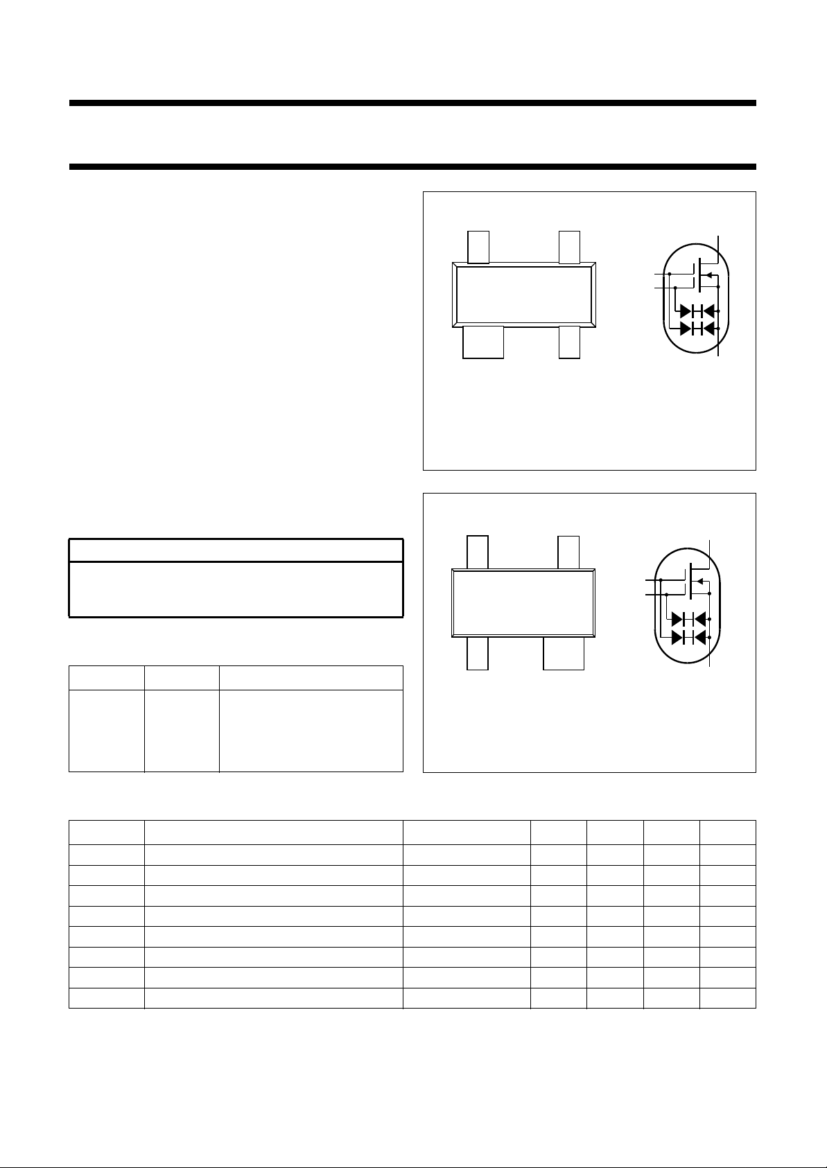
handbook, halfpage
Top view
Fig.1 Simplified outline (SOT143) and
handbook, halfpage
43
21
symbol; BF908.
34
MAM039
g
g
d
g
2
g
1
s,b
d
2
1
PINNING
PIN SYMBOL DESCRIPTION
Top view
12
MAM040
s,b
1 s, b source
2 d drain
3g
4g
2
1
gate 2
gate 1
Fig.2 Simplified outline (SOT143R) and
symbol; BF908R.
QUICK REFERENCE DATA
SYMBOL PARAMETER CONDITIONS MIN. TYP. MAX. UNIT
V
DS
I
D
P
tot
T
j
forward transfer admittance 36 43 50 mS
y
fs
C
ig1-s
C
rs
drain-source voltage −−12 V
drain current −−40 mA
total power dissipation −−200 mW
operating junction temperature −−150 °C
input capacitance at gate 1 2.4 3.1 4 pF
reverse transfer capacitance f = 1 MHz 20 30 45 pF
F noise figure f = 800 MHz − 1.5 2.5 dB
1996 Jul 30 2
Page 3
Philips Semiconductors Product specification
Dual-gate MOS-FETs BF908; BF908R
LIMITING VALUES
In accordance with the Absolute Maximum Rating System (IEC 134).
SYMBOL PARAMETER CONDITIONS MIN. MAX. UNIT
V
DS
I
D
±I
G1
±I
G2
P
tot
T
stg
T
j
Note
1. Device mounted on a printed-circuit board.
drain-source voltage − 12 V
drain current − 40 mA
gate 1 current − 10 mA
gate 2 current − 10 mA
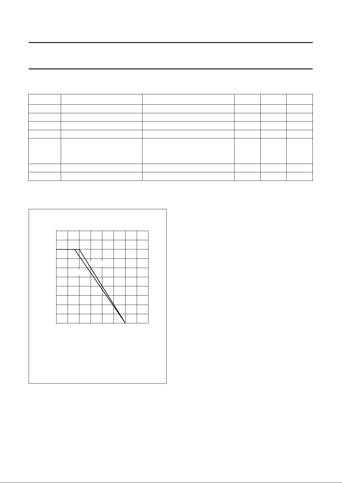
total power dissipation see Fig.3; note 1
BF908 up to T
BF908R up to T
=50°C − 200 mW
amb
=40°C − 200 mW
amb
storage temperature −65 +150 °C
operating junction temperature − 150 °C
250
handbook, halfpage
P
tot
(mW)
200
150
100
50
0
0 50 100 150 200
BF908
BF908R
T
Fig.3 Power derating curves.
amb
MRC275
o
( C)
1996 Jul 30 3
Page 4

Philips Semiconductors Product specification
Dual-gate MOS-FETs BF908; BF908R
THERMAL CHARACTERISTICS
SYMBOL PARAMETER CONDITIONS VALUE UNIT
R
th j-a
Note
1. Device mounted on a printed-circuit board.
STATIC CHARACTERISTICS
=25°C; unless otherwise specified.
T
j
SYMBOL PARAMETER CONDITIONS MIN. TYP. MAX. UNIT
±V
(BR)G1-SS
±V
(BR)G2-SS
−V
(P)G1-S
−V
(P)G2-S
I
DSS
±I
G1-SS
±I
G2-SS
thermal resistance from junction to ambient note 1
BF908 500 K/W
BF908R 550 K/W
gate 1-source breakdown voltage V
gate 2-source breakdown voltage V
gate 1-source cut-off voltage V
gate 2-source cut-off voltage V
drain-source current V
gate 1 cut-off current V
gate 2 cut-off current V
G2-S=VDS
G1-S=VDS
G2-S
G1-S
G2-S
G2-S=VDS
G1-S=VDS
= 0; I
= 0; I
=10mA 8 − 20 V
G1-S
=10mA 8 − 20 V
G2-S
=4V; VDS=8V; ID=20µA −−2V
=4V; VDS=8V; ID=20µA −−1.5 V
=4V; VDS=8V; V
= 0; V
G1-S
= 0; V
G2-S
=03 1527mA
G1-S
=5V −−50 nA
=5V −−50 nA
DYNAMIC CHARACTERISTICS
Common source; T
=25°C; VDS=8V; V
amb
=4V; ID= 15 mA; unless otherwise specified.
G2-S
SYMBOL PARAMETER CONDITIONS MIN. TYP. MAX. UNIT
y
forward transfer admittance pulsed; Tj=25°C; f = 1 MHz 36 43 50 mS
fs
C
ig1-s
C
ig2-s
C
os
C
rs
F noise figure f = 200 MHz; G
input capacitance at gate 1 f = 1 MHz 2.4 3.1 4 pF
input capacitance at gate 2 f = 1 MHz 1.2 1.8 2.5 pF
output capacitance f = 1 MHz 1.2 1.7 2.2 pF
reverse transfer capacitance f = 1 MHz 20 30 45 fF
f = 800 MHz; G
= 2 mS; BS=B
S
S=GSopt
; BS=B
Sopt
Sopt
− 0.6 1.2 dB
− 1.5 2.5 dB
1996 Jul 30 4
Page 5

Philips Semiconductors Product specification
Dual-gate MOS-FETs BF908; BF908R
40
handbook, halfpage
ID
(mA)
30
20
10
0
−0.6 −0.4 0 0.2−0.2 0.4
VDS= 8V; Tj=25°C.
V
V
G2-S
G1-S
Fig.4 Transfer characteristics; typical values.
MRC281
= 4 V
3 V
2 V
1.5 V
1 V
0.5 V
0 V
(V)
0.6
30
handbook, halfpage
ID
(mA)
20
10
0
048 16
V
= 4 V; Tj=25°C.
G2-S
V
G1-S
12
Fig.5 Output characteristics; typical values.
MRC282
= 0.3 V
0.2 V
0.1 V
0 V
−0.1 V
−0.2 V
−0.3 V
VDS (V)
50
Y
fs
(mS)
40
30
20
10
V
G2-S
0
0 5 10 15 20 25
VDS= 8 V; Tj=25°C.
0.5 V
= 0 V
MRC280
4 V
3 V
2 V
1.5 V
1 V
ID(mA)
Fig.6 Forward transfer admittance as a function
of drain current; typical values.
60
Y
fs
(mS)
40
20
0
VDS= 8 V; V
0 40 80 120 16040
= 4 V; ID=15mA.
G2-S
MRC276
o
Tj( C)
Fig.7 Forward transfer admittance as a function
of junction temperature; typical values.
1996 Jul 30 5
Page 6

Philips Semiconductors Product specification
Dual-gate MOS-FETs BF908; BF908R
Table 1 Scattering parameters
f
(MHz)
V
DS
MAGNITUDE
=8V; V
s
11
ANGLE
(ratio)
=4V; ID= 10 mA; T
G2-S
MAGNITUDE
(deg)
amb
(ratio)
=25°C.
s
21
ANGLE
MAGNITUDE
(deg)
(ratio)
s
12
ANGLE
MAGNITUDE
(deg)
(ratio)
s
22
ANGLE
(deg)
50 0.998 −5.1 3.537 173.5 0.001 98.2 0.996 −2.4
100 0.994 −10.4 3.502 167.7 0.001 88.8 0.994 −4.9
200 0.979 −20.8 3.450 154.9 0.003 74.6 0.987 −9.5
300 0.962 −30.3 3.318 143.7 0.004 69.5 0.983 −13.9
400 0.939 −40.1 3.234 131.9 0.005 65.6 0.980 −18.5
500 0.914 −49.1 3.093 120.7 0.006 64.4 0.974 −22.8
600 0.892 −57.1 2.912 111.1 0.005 63.1 0.969 −27.0
700 0.865 −64.4 2.774 101.0 0.005 65.2 0.966 −31.2
800 0.837 −71.6 2.616 91.4 0.004 70.8 0.965 −35.4
900 0.811 −78.1 2.479 81.9 0.004 87.4 0.965 −39.4
1000 0.785 −84.5 3.329 72.5 0.003 108.0 0.966 −43.7
V
DS
=8V; V
=4V; ID= 15 mA; T
G2-S
amb
=25°C.
50 0.998 −5.3 3.983 173.4 0.001 95.5 0.994 −2.4
100 0.994 −10.9 3.943 167.5 0.001 93.6 0.991 −5.0
200 0.976 −21.6 3.878 154.7 0.003 74.3 0.984 −9.7
300 0.957 −31.7 3.722 143.3 0.004 70.0 0.979 −14.2
400 0.934 −41.7 3.614 131.6 0.005 63.5 0.975 −18.8
500 0.907 −51.1 3.446 120.4 0.006 62.2 0.969 −23.2
600 0.885 −59.1 3.240 110.9 0.005 59.6 0.964 −27.4
700 0.851 −66.8 3.072 100.9 0.005 64.8 0.961 −31.6
800 0.826 −73.9 2.891 91.3 0.004 67.8 0.959 −35.9
900 0.797 −80.7 2.733 81.9 0.004 85.0 0.958 −40.0
1000 0.773 −87.0 2.569 72.8 0.004 102.9 0.958 −44.2
Table 2 Noise data
V
DS
f
(MHz)
=8V; V
=4V; ID= 10 mA; T
G2-S
F
min
(dB)
amb
=25°C.
800 1.50 0.720 56.7 0.580
V
=8V; V
DS
=4V; ID= 15 mA; T
G2-S
amb
=25°C.
800 1.50 0.700 59.2 0.520
1996 Jul 30 6
Γ
opt
(ratio) (deg)
r
n
Page 7

Philips Semiconductors Product specification
Dual-gate MOS-FETs BF908; BF908R
PACKAGE OUTLINES
handbook, full pagewidth
Dimensions in mm.
10
max
3.0
0.150
30
max
0.090
0.1
max
max
o
o
10
0.88
0.75
0.60
o
1.1
max
2.8
1.9
43
1
2
0
0.1
TOP VIEW
0.48
1.7
0
0.1
B
A
1.4
1.2
M0.1 AB
2.5
max
0.2
MBC845
M
AB
Fig.8 SOT143.
handbook, full pagewidth
Dimensions in mm.
0.40
0.25
10
max
3.0
0.150
0.090
30
max
o
0.1
max
10
max
o
0.48
0.38
o
1.1
max
2.8
1.9
34
2
1
0.88
0.78
1.7
M0.1 B
TOP VIEW
B
A
1.4
1.2
MBC844
2.5
max
0.2
A
M
Fig.9 SOT143R.
1996 Jul 30 7
Page 8

Philips Semiconductors Product specification
Dual-gate MOS-FETs BF908; BF908R
DEFINITIONS
Data Sheet Status
Objective specification This data sheet contains target or goal specifications for product development.
Preliminary specification This data sheet contains preliminary data; supplementary data may be published later.
Product specification This data sheet contains final product specifications.
Limiting values
Limiting values given are in accordance with the Absolute Maximum Rating System (IEC 134). Stress above one or
more of the limiting values may cause permanent damage to the device. These are stress ratings only and operation
of the device at these or at any other conditions above those given in the Characteristics sections of the specification
is not implied. Exposure to limiting values for extended periods may affect device reliability.
Application information
Where application information is given, it is advisory and does not form part of the specification.
LIFE SUPPORT APPLICATIONS
These products are not designed for use in life support appliances, devices, or systems where malfunction of these
products can reasonably be expected to result in personal injury. Philips customers using or selling these products for
use in such applications do so at their own risk and agree to fully indemnify Philips for any damages resulting from such
improper use or sale.
1996 Jul 30 8
 Loading...