

Page 1

DISCRETE SEMICONDUCTORS
DATA SH EET
BF904; BF904R
N-channel dual gate MOS-FETs
Product specification
Supersedes data of 1997 Sep 05
1999 May 17
Page 2
Philips Semiconductors Product specification
N-channel dual gate MOS-FETs BF904; BF904R
FEATURES
• Specially designed for use at 5 V supply voltage
• Short channel transistor with high transfer admittance to
input capacitance ratio
• Low noise gain controlled amplifier up to 1 GHz
• Superior cross-modulation performance during AGC.
APPLICATIONS
• VHF and UHF applications with 3 to 7 V supply voltage
such as television tuners and professional
communications equipment.
DESCRIPTION
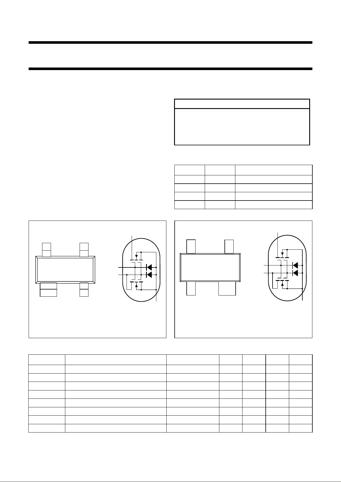
Enhancement type field-effect transistor in a plastic
microminiature SOT143B and SOT143R package. The
transistor consists of an amplifier MOS-FET with source
handbook, halfpage
43
d
and substrate interconnected and an internal bias circuit to
ensure good cross-modulation performance during AGC.
CAUTION
This product is supplied in anti-static packing to
prevent damage caused by electrostatic discharge
during transport and handling. For further information,
refer to Philips specs.: SNW-EQ-608, SNW-FQ-302A
and SNW-FQ-302B.
PINNING
PIN SYMBOL DESCRIPTION
1 s, b source
2 d drain
3g
4g
handbook, halfpage
34
gate 2
2
gate 1
1
d
g
2
g
1
21
Top view
BF904 marking code: M04.
MAM124
Fig.1 Simplified outline (SOT143B) and symbol.
s,b
12
Top view
BF904R marking code: M06.
MAM125 - 1
Fig.2 Simplified outline (SOT143R) and symbol.
g
2
g
1
QUICK REFERENCE DATA
SYMBOL PARAMETER CONDITIONS MIN. TYP. MAX. UNIT
V
DS
I
D
P
tot
T
j
forward transfer admittance 22 25 30 mS
y
fs
C
ig1-s
C
rs
drain-source voltage −−7V
drain current −−30 mA
total power dissipation −−200 mW
operating junction temperature −−150 °C
input capacitance at gate 1 − 2.2 2.6 pF
reverse transfer capacitance f = 1 MHz − 25 35 fF
F noise figure f = 800 MHz − 2 − dB
s,b
1999 May 17 2
Page 3
Philips Semiconductors Product specification
N-channel dual gate MOS-FETs BF904; BF904R
LIMITING VALUES
In accordance with the Absolute Maximum Rating System (IEC 134).
SYMBOL PARAMETER CONDITIONS MIN. MAX. UNIT
V
DS
I
D
I
G1
I
G2
P
tot
T
stg
T
j
Note
1. Device mounted on a printed-circuit board.
drain-source voltage − 7V
drain current − 30 mA
gate 1 current −±10 mA
gate 2 current −±10 mA
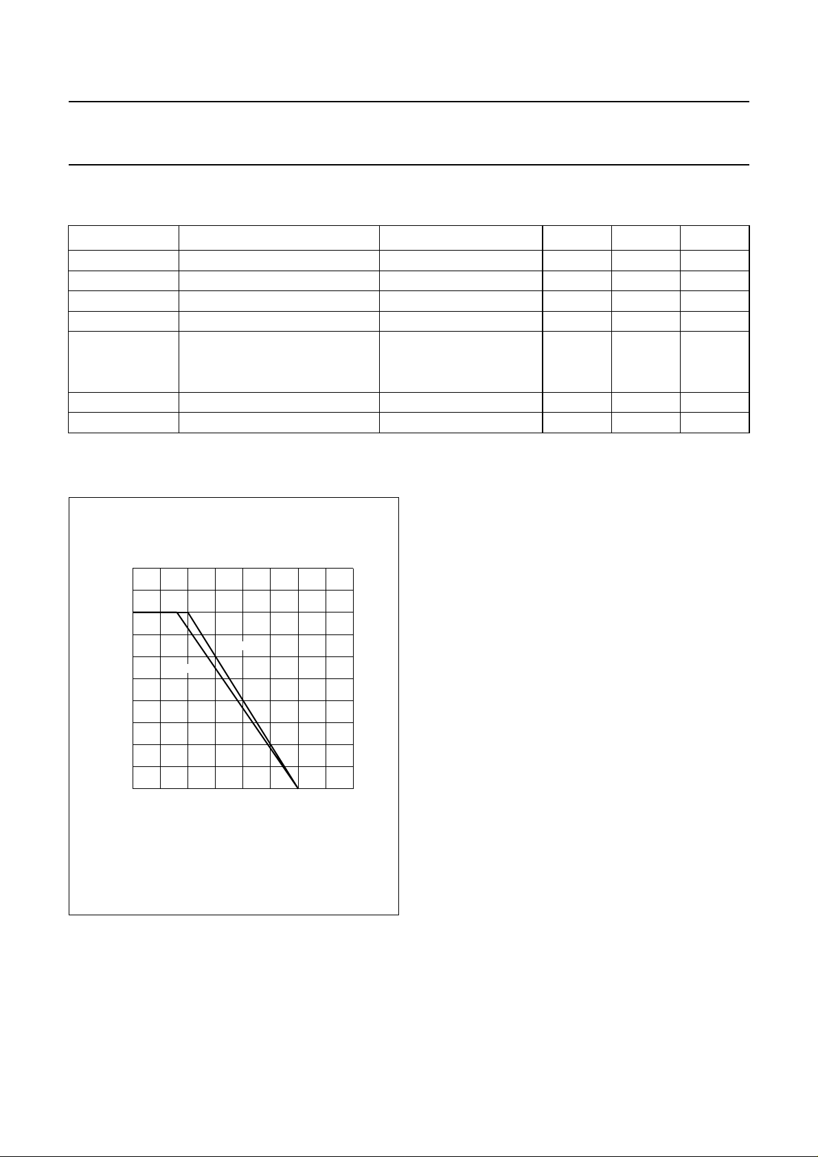
total power dissipation see Fig.3
BF904 T
BF904R T
≤ 50 °C; note 1 − 200 mW
amb
≤ 40 °C; note 1 − 200 mW
amb
storage temperature −65 +150 °C
operating junction temperature − 150 °C
250
handbook, halfpage
P
tot
(mW)
200
150
100
50
0
0 50 100 150 200
BF904
BF904R
T
Fig.3 Power derating curves.
amb
MRA770
o
( C)
1999 May 17 3
Page 4
Philips Semiconductors Product specification
N-channel dual gate MOS-FETs BF904; BF904R
THERMAL CHARACTERISTICS
SYMBOL PARAMETER CONDITIONS VALUE UNIT
R
th j-a
R
th j-s
Notes
1. Device mounted on a printed-circuit board.
is the temperature at the soldering point of the source lead.
2. T
s
STATIC CHARACTERISTICS
Tj=25°C unless otherwise specified.
thermal resistance from junction to ambient note 1
BF904 500 K/W
BF904R 550 K/W
thermal resistance from junction to soldering point note 2
BF904 T
BF904R T
=92°C 290 K/W
s
=78°C 360 K/W
s
SYMBOL PARAMETER CONDITIONS MIN. MAX. UNIT
V
(BR)G1-SS
V
(BR)G2-SS
V
(F)S-G1
V
(F)S-G2
V
G1-S(th)
V
G2-S(th)
I
DSX
gate 1-source breakdown voltage V
gate 2-source breakdown voltage V
forward source-gate 1 voltage V
forward source-gate 2 voltage V
gate 1-source threshold voltage V
gate 2-source threshold voltage V
drain-source current V
G2-S=VDS
G1-S=VDS
G2-S=VDS
G1-S=VDS
G2-S
G1-S=VDS
G2-S
= 0; I
= 0; I
= 0; I
= 0; I
= 10 mA 6 15 V
G1-S
= 10 mA 6 15 V
G2-S
= 10 mA 0.5 1.5 V
S-G1
= 10 mA 0.5 1.5 V
S-G2
=4V; VDS=5V; ID=20µA 0.3 1 V
=5V; ID=20µA 0.3 1.2 V
=4V; VDS=5V;
813mA
RG1= 120 kΩ; note 1
I
G1-SS
I
G2-SS
gate 1 cut-off current V
gate 2 cut-off current V
G2-S=VDS
G1-S=VDS
= 0; V
= 0; V
=5V − 50 nA
G1-S
=5V − 50 nA
G2-S
Note
1. R
connects gate 1 to VGG= 5 V; see Fig.20.
G1
DYNAMIC CHARACTERISTICS
Common source; T
=25°C; VDS= 5 V; V
amb
= 4 V; ID= 10 mA; unless otherwise specified.
G2-S
SYMBOL PARAMETER CONDITIONS MIN. TYP. MAX. UNIT
forward transfer admittance pulsed; Tj=25°C 222530mS
y
fs
C
ig1-s
C
ig2-s
C
os
C
rs
F noise figure f = 200 MHz; G
input capacitance at gate 1 f = 1 MHz − 2.2 2.6 pF
input capacitance at gate 2 f = 1 MHz 1 1.5 2 pF
drain-source capacitance f = 1 MHz 1 1.3 1.6 pF
reverse transfer capacitance f = 1 MHz − 25 35 fF
f = 800 MHz; G
= 2 mS; BS=B
S
S=GSopt
; BS=B
− 1 1.5 dB
Sopt
− 2 2.8 dB
Sopt
1999 May 17 4
Page 5
Philips Semiconductors Product specification
N-channel dual gate MOS-FETs BF904; BF904R
100
MLD268
o
T ( C)
j
40
Y
fs
(mS)
30
20
10
0
50 0 50 150
Fig.4 Transfer admittance as a function of the
junction temperature; typical values.
gain
(dB)
10
20
30
40
50
f =50 MHz.
0
01234
handbook, halfpage
reduction
Fig.5 Typical gain reduction as a function of
the AGC voltage.
MRA769
V (V)
AGC
120
handbook, halfpage
V
unw
(dB V)
µ
110
100
90
80
0 1020304050
VDS= 5 V; VGG= 5 V; fw= 50 MHz.
f
= 60 MHz; T
unw
=25°C; RG1= 120 kΩ.
amb
gain reduction (dB)
MRA771
Fig.6 Unwanted voltage for 1% cross-modulation
as a function of gain reduction; typical
values; see Fig.20.
20
I
D
(mA)
15
10
VDS=5V.
Tj=25°C.
5
0
0
0.4 2.0
V = 4 V
G2 S
0.8 1.2 1.6
3 V 2.5 V
V (V)
Fig.7 Transfer characteristics; typical values.
MLD270
2 V
1.5 V
1 V
G1 S
1999 May 17 5
Page 6

Philips Semiconductors Product specification
N-channel dual gate MOS-FETs BF904; BF904R
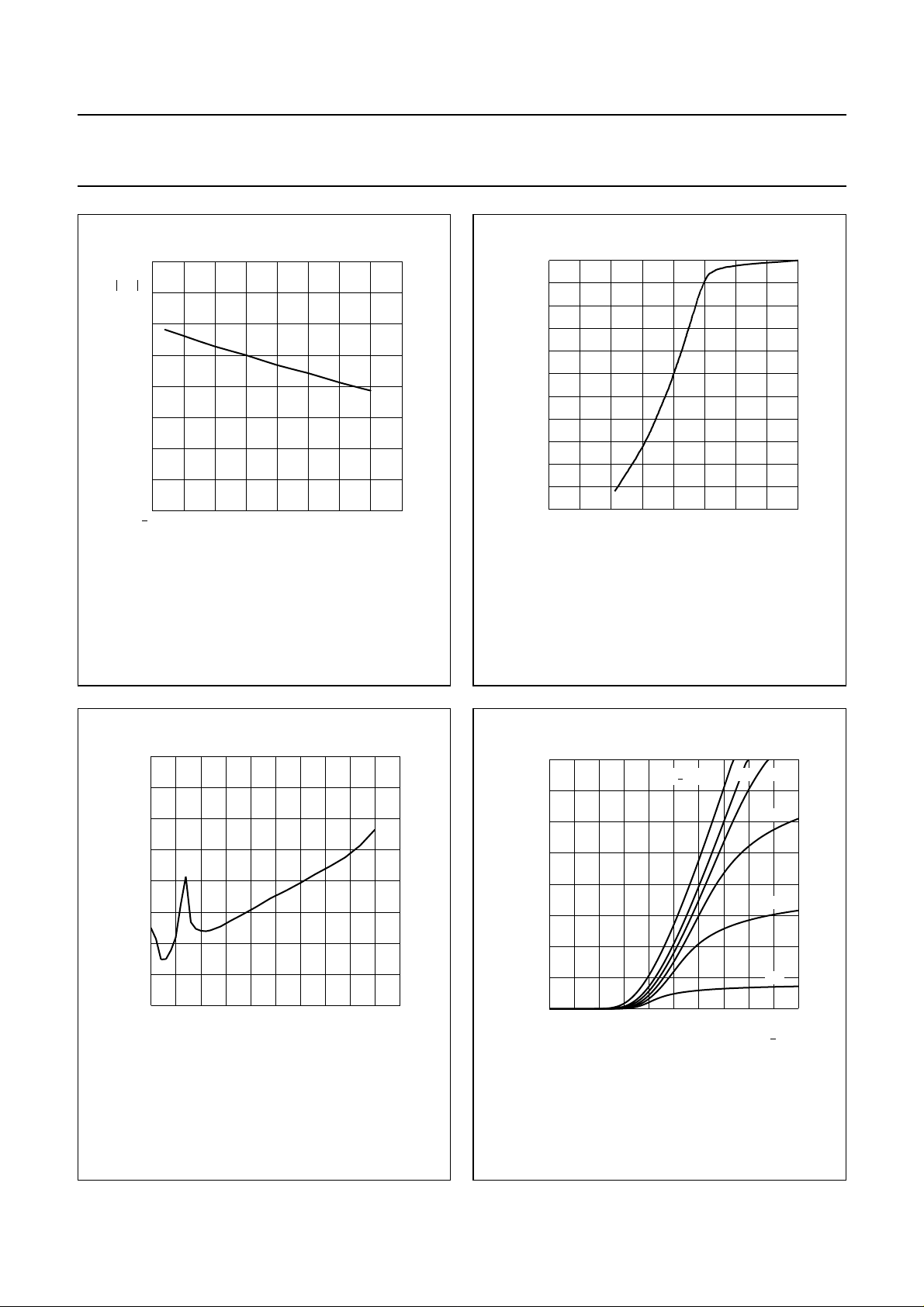
20
handbook, halfpage
I
D
(mA)
16
12
8
4
0
0
V
=4V.
G2-S
Tj=25°C.
210
V = 1.4 V
G1 S
1.3 V
1.2 V
1.1 V
1.0 V
0.9 V
468
Fig.8 Output characteristics; typical values.
MLD269
V (V)
DS
150
handbook, halfpage
I
G1
(µA)
100
50
0
0
VDS=5V.
Tj=25°C.
0.5 2.5
1.0 1.5 2.0
V = 4 V
G2 S
Fig.9 Gate 1 current as a function of gate 1
voltage; typical values.
MLD271
3.5 V
3 V
2.5 V
2 V
V (V)
G1 S
40
handbook, halfpage
y
fs
(mS)
30
20
10
0
0
VDS=5V.
Tj=25°C.
4 8 12 16 20
Fig.10 Forward transfer admittance as a
function of drain current; typical values.
MLD272
V = 4 V
G2 S
3.5 V
3 V
2.5 V
2 V
I (mA)
D
16
handbook, halfpage
I
D
(mA)
12
8
4
0
0
VDS=5V.
V
=4V.
G2-S
Tj=25°C.
10 50
20 30 40
MLD273
I (µA)
G1
Fig.11 Drain current as a function of gate 1 current;
typical values.
1999 May 17 6
Page 7

Philips Semiconductors Product specification
N-channel dual gate MOS-FETs BF904; BF904R
12
handbook, halfpage
I
D
(mA)
8
4
0
0
VDS= 5 V; V
RG1= 120 kΩ (connected to VGG); Tj=25°C.
15
=4V.
G2-S
234
Fig.12 Drain current as a function of gate 1
supply voltage (= VGG); typical values;
see Fig.20.
MLD275
V (V)
GG
20
handbook, halfpage
I
D
(mA)
15
10
5
0
0
V
=4V.
G2-S
RG1 connected to VGG; Tj=25°C.
R = 47 kΩ
24 8
G1
68 kΩ
V = V (V)
GG DS
Fig.13 Drain current as a function of gate 1
(= VGG) and drain supply voltage;
typical values; see Fig.20.
MLD274
82 kΩ
100 kΩ
120 kΩ
150 kΩ
180 kΩ
220 kΩ
6
12
handbook, halfpage
I
D
(mA)
8
4
0
0246
VDS= 5 V; Tj=25°C.
RG1= 120 kΩ (connected to VGG).
V = 5 V
GG
4.5 V
4 V
3.5 V
3 V
V (V)
G2 S
MLD276
Fig.14 Drain current as a function of gate 2 voltage;
typical values; see Fig.20.
40
handbook, halfpage
I
G1
(µA)
30
20
10
0
0246
VDS= 5 V; Tj=25°C.
RG1= 120 kΩ (connected to VGG).
V = 5 V
GG
V (V)
Fig.15 Gate 1 current as a function of gate 2
voltage; typical values; see Fig.20.
MLB945
4.5 V
4 V
3.5 V
3 V
G2 S
1999 May 17 7
Page 8

Philips Semiconductors Product specification
N-channel dual gate MOS-FETs BF904; BF904R
2
10
handbook, halfpage
y
is
MLD277
(mS)
10
b
is
1
g
is
1
10
10
2
10
f (MHz)
VDS= 5 V; VG2=4V.
ID= 15 mA; T
amb
=25°C.
Fig.16 Input admittance as a function of frequency;
typical values.
f (MHz)
MLD278
3
10
ϕ
rs
(deg)
2
10
10
1
3
10
3
10
y
rs
(µS)
ϕ
2
10
rs
y
rs
10
3
10
1
10
2
10
VDS= 5 V; VG2=4V.
ID= 15 mA; T
amb
=25°C.
Fig.17 Reverse transfer admittance and phase as
a function of frequency; typical values.
MLD279
3
10
y
(mS)
2
10
fs
10
1
10
y
fs
ϕ
fs
2
10
f (MHz)
VDS= 5 V; VG2=4V.
ID= 15 mA; T
amb
=25°C.
Fig.18 Forward transfer admittance and phase as
a function of frequency; typical values.
10
ϕ
(deg)
10
1
2
fs
10
handbook, halfpage
y
os
(mS)
b
os
MLD280
1
g
1
10
2
10
10
os
2
10
f (MHz)
3
10
VDS= 5 V; VG2=4V.
ID= 15 mA; T
amb
=25°C.
Fig.19 Output admittance as a function of
frequency; typical values.
1999 May 17 8
Page 9

Philips Semiconductors Product specification
N-channel dual gate MOS-FETs BF904; BF904R
V
AGC
R1
10 kΩ
C1
R
GEN
50
V
4.7 nF
C2
4.7 nF
R2
50
Ω
I
Ω
R
G1
V
GG
DUT
V
DS
C3 12 pF
L1
450 nH
≈
C4
4.7 nF
R
50 Ω
MLD171
L
Fig.20 Cross-modulation test set-up.
1999 May 17 9
Page 10

Philips Semiconductors Product specification
N-channel dual gate MOS-FETs BF904; BF904R
Table 1 Scattering parameters:VDS=5 V; V
S
f
(MHz)
MAGNITUDE
(ratio)
11
ANGLE
(deg)
MAGNITUDE
(ratio)
= 4 V; ID=10mA
G2-S
S
21
ANGLE
(deg)
S
12
MAGNITUDE
(ratio)
ANGLE
(deg)
S
MAGNITUDE
(ratio)
22
ANGLE
(deg)
40 0.989 −3.4 2.420 175.7 0.000 79.9 0.993 −1.6
100 0.985 −8.3 2.414 169.1 0.001 78.3 0.992 −3.9
200 0.976 −16.4 2.368 158.8 0.003 80.3 0.987 −7.8
300 0.958 −24.1 2.301 148.5 0.004 73.7 0.980 −11.4
400 0.942 −32.0 2.251 138.8 0.005 70.7 0.974 −15.2
500 0.918 −39.3 2.170 129.5 0.005 67.2 0.966 −18.7
600 0.899 −46.0 2.080 120.7 0.005 67.8 0.958 −22.2
700 0.876 −52.6 2.001 112.1 0.005 68.6 0.951 −25.5
800 0.852 −58.8 1.924 103.2 0.005 72.9 0.944 −28.9
900 0.823 −64.9 1.829 94.7 0.005 78.7 0.937 −32.1
1000 0.800 −70.9 1.747 86.5 0.005 88.3 0.933 −35.2
1200 0.750 −82.4 1.621 70.7 0.005 120.5 0.928 −41.7
1400 0.719 −92.7 1.535 54.6 0.008 139.8 0.930 −48.4
1600 0.682 −102.5 1.424 39.4 0.010 137.8 0.924 −54.9
1800 0.642 −109.8 1.349 22.5 0.013 156.8 0.928 −62.9
2000 0.602 −116.5 1.283 1.1 0.018 175.1 0.928 −73.1
2200 0.547 −124.9 1.130 −15.1 0.014 172.6 0.887 −81.0
2400 0.596 −128.7 1.018 −49.1 0.040 −163.9 0.837 −95.8
2600 0.682 −132.6 0.979 −79.4 0.077 −164.0 0.778 −109.6
2800 0.771 −142.5 0.804 −116.2 0.120 178.8 0.629 −119.5
3000 0.793 −157.5 0.541 −153.5 0.149 158.3 0.479 −119.9
Table 2 Noise data:V
f
(MHz)
DS
= 5 V; V
= 4 V; ID=10mA
G2-S
F
min
(dB)
800 2.00 0.686 49.6 50.40
1999 May 17 10
Γ
opt
(ratio) (deg)
r
n
Page 11

Philips Semiconductors Product specification
N-channel dual gate MOS-FETs BF904; BF904R
PACKAGE OUTLINES
Plastic surface mounted package; 4 leads SOT143B
D
y
e
b
p
B
w M
E
v M
A
B
H
E
A
X
34
Q
A
A
1
21
b
1
e
1
detail X
L
c
p
0 1 2 mm
scale
DIMENSIONS (mm are the original dimensions)
A
UNIT
mm
1.1
0.9
OUTLINE
VERSION
SOT143B
1
A
max
0.1
b
c
D
b
0.48
0.38
1
p
0.88
0.15
0.78
0.09
IEC JEDEC EIAJ
E
3.0
1.4
2.8
1.2
REFERENCES
e
1.9
1999 May 17 11
e
1.7
H
L
E
1
2.5
2.1
0.45
0.15
p
0.55
0.45
EUROPEAN
PROJECTION
ywvQ
0.1 0.10.2
ISSUE DATE
97-02-28
Page 12

Philips Semiconductors Product specification
N-channel dual gate MOS-FETs BF904; BF904R
Plastic surface mounted package; reverse pinning; 4 leads SOT143R
D
y
e
b
p
B
w M
E
v M
A
B
H
E
A
X
43
Q
A
A
1
c
12
L
b
1
e
1
detail X
p
0 1 2 mm
scale
DIMENSIONS (mm are the original dimensions)
A
UNIT
mm
1.1
0.9
OUTLINE
VERSION
SOT143R
1
A
max
0.1
b
c
D
b
0.48
0.38
1
p
0.88
0.15
0.78
0.09
IEC JEDEC EIAJ
E
3.0
1.4
2.8
1.2
REFERENCES
e
1.9
1999 May 17 12
e
1.7
H
L
E
1
2.5
2.1
0.55
0.25
p
0.45
0.25
EUROPEAN
PROJECTION
ywvQ
0.1 0.10.2
ISSUE DATE
97-03-10
Page 13

Philips Semiconductors Product specification
N-channel dual gate MOS-FETs BF904; BF904R
DEFINITIONS
Data Sheet Status
Objective specification This data sheet contains target or goal specifications for product development.
Preliminary specification This data sheet contains preliminary data; supplementary data may be published later.
Product specification This data sheet contains final product specifications.
Limiting values
Limiting values given are in accordance with the Absolute Maximum Rating System (IEC 134). Stress above one or
more of the limiting values may cause permanent damage to the device. These are stress ratings only and operation
of the device at these or at any other conditions above those given in the Characteristics sections of the specification
is not implied. Exposure to limiting values for extended periods may affect device reliability.
Application information
Where application information is given, it is advisory and does not form part of the specification.
LIFE SUPPORT APPLICATIONS
These products are not designed for use in life support appliances, devices, or systems where malfunction of these
products can reasonably be expected to result in personal injury. Philips customers using or selling these products for
use in such applications do so at their own risk and agree to fully indemnify Philips for any damages resulting from such
improper use or sale.
1999 May 17 13
Page 14

Philips Semiconductors Product specification
N-channel dual gate MOS-FETs BF904; BF904R
NOTES
1999 May 17 14
Page 15

Philips Semiconductors Product specification
N-channel dual gate MOS-FETs BF904; BF904R
NOTES
1999 May 17 15
Page 16

Philips Semiconductors – a worldwide company
Argentina: see South America
Australia: 34 Waterloo Road, NORTH RYDE, NSW 2113,
Tel. +61 2 9805 4455, Fax. +61 29805 4466
Austria: Computerstr. 6, A-1101 WIEN, P.O. Box 213,
Tel. +43 1 60 101 1248, Fax. +43 1 60 1011210
Belarus: Hotel Minsk Business Center, Bld. 3, r. 1211, Volodarski Str. 6,
220050 MINSK, Tel. +375 172 20 0733, Fax. +375 172 200773
Belgium: see The Netherlands
Brazil: seeSouth America
Bulgaria: Philips Bulgaria Ltd., Energoproject, 15thfloor,
51 James Bourchier Blvd., 1407 SOFIA,
Tel. +359 2 68 9211, Fax. +359 268 9102
Canada: PHILIPS SEMICONDUCTORS/COMPONENTS,
Tel. +1 800 234 7381, Fax. +1 800 9430087
China/Hong Kong: 501 Hong Kong Industrial Technology Centre,
72 Tat Chee Avenue, Kowloon Tong, HONG KONG,
Tel. +852 2319 7888, Fax. +8522319 7700
Colombia: see South America
Czech Republic: see Austria
Denmark: Sydhavnsgade 23, 1780 COPENHAGEN V,
Tel. +45 33 29 3333, Fax. +45 33 29 3905
Finland: Sinikalliontie 3, FIN-02630 ESPOO,
Tel. +358 9 615 800, Fax. +358 96158 0920
France: 51 Rue Carnot, BP317, 92156 SURESNES Cedex,
Tel. +33 1 4099 6161, Fax. +33 14099 6427
Germany: Hammerbrookstraße 69, D-20097 HAMBURG,
Tel. +49 40 2353 60, Fax. +49 40 2353 6300
Hungary: seeAustria
India: Philips INDIA Ltd, Band Box Building, 2nd floor,
254-D, Dr. Annie BesantRoad, Worli, MUMBAI 400 025,
Tel. +91 22 493 8541, Fax.+91 22493 0966
Indonesia: PT Philips Development Corporation, Semiconductors Division,
Gedung Philips, Jl. Buncit Raya Kav.99-100, JAKARTA 12510,
Tel. +62 21 794 0040 ext.2501, Fax. +6221 7940080
Ireland: Newstead, Clonskeagh, DUBLIN 14,
Tel. +353 1 7640 000, Fax.+353 17640 200
Israel: RAPAC Electronics, 7 Kehilat Saloniki St, PO Box 18053,
TEL AVIV 61180, Tel. +972 3 645 0444, Fax.+972 3649 1007
Italy: PHILIPS SEMICONDUCTORS, Piazza IV Novembre 3,
20124 MILANO, Tel. +39 02 67 52 2531, Fax. +39 02 67 522557
Japan: Philips Bldg 13-37, Kohnan 2-chome, Minato-ku,
TOKYO 108-8507, Tel. +81 3 3740 5130, Fax. +81 3 3740 5077
Korea: Philips House, 260-199 Itaewon-dong, Yongsan-ku, SEOUL,
Tel. +82 2 709 1412, Fax. +82 2 709 1415
Malaysia: No. 76 Jalan Universiti, 46200 PETALING JAYA, SELANGOR,
Tel. +60 3 750 5214, Fax. +60 3 7574880
Mexico: 5900 Gateway East, Suite 200, EL PASO, TEXAS 79905,
Tel. +9-5 800 234 7381, Fax +9-5800 9430087
Middle East: see Italy
Netherlands: Postbus 90050, 5600 PB EINDHOVEN, Bldg. VB,
Tel. +31 40 27 82785, Fax. +31 4027 88399
New Zealand: 2 Wagener Place, C.P.O. Box 1041, AUCKLAND,
Tel. +64 9 849 4160, Fax. +64 9 849 7811
Norway: Box 1, Manglerud 0612, OSLO,
Tel. +47 22 74 8000, Fax. +47 22 74 8341
Pakistan: see Singapore
Philippines: Philips Semiconductors Philippines Inc.,
106 Valero St. Salcedo Village, P.O. Box 2108 MCC,MAKATI,
Metro MANILA, Tel. +63 2 816 6380, Fax. +632 817 3474
Poland: Ul. Lukiska 10, PL 04-123 WARSZAWA,
Tel. +48 22 612 2831, Fax.+48 22612 2327
Portugal: see Spain
Romania: see Italy
Russia: Philips Russia, Ul. Usatcheva 35A, 119048 MOSCOW,
Tel. +7 095 755 6918, Fax.+7 095755 6919
Singapore: Lorong 1, Toa Payoh, SINGAPORE 319762,
Tel. +65 350 2538, Fax. +65 251 6500
Slovakia: see Austria
Slovenia: see Italy
South Africa: S.A. PHILIPS Pty Ltd., 195-215 Main Road Martindale,
2092 JOHANNESBURG, P.O. Box 58088 Newville 2114,
Tel. +27 11 471 5401, Fax.+27 11471 5398
South America: Al. Vicente Pinzon, 173, 6th floor,
04547-130 SÃO PAULO, SP, Brazil,
Tel. +55 11 821 2333, Fax.+55 11821 2382
Spain: Balmes 22, 08007 BARCELONA,
Tel. +34 93 301 6312, Fax.+34 93301 4107
Sweden: Kottbygatan 7, Akalla, S-16485 STOCKHOLM,
Tel. +46 8 5985 2000, Fax. +46 85985 2745
Switzerland: Allmendstrasse 140, CH-8027 ZÜRICH,
Tel. +41 1 488 2741 Fax. +41 1 488 3263
Taiwan: Philips Semiconductors, 6F, No. 96, Chien Kuo N. Rd., Sec. 1,
TAIPEI, Taiwan Tel. +886 2 2134 2886, Fax. +886 2 2134 2874
Thailand: PHILIPS ELECTRONICS (THAILAND) Ltd.,
209/2 Sanpavuth-Bangna Road Prakanong, BANGKOK 10260,
Tel. +66 2 745 4090, Fax. +66 2 398 0793
Turkey: Yukari Dudullu, Org. San. Blg., 2.Cad. Nr. 28 81260 Umraniye,
ISTANBUL, Tel. +90 216 522 1500, Fax. +90 216522 1813
Ukraine: PHILIPS UKRAINE, 4 Patrice Lumumba str., Building B, Floor 7,
252042 KIEV, Tel. +380 44 264 2776, Fax. +38044 268 0461
United Kingdom: Philips Semiconductors Ltd., 276 Bath Road, Hayes,
MIDDLESEX UB3 5BX, Tel. +44 181 730 5000, Fax.+44 181754 8421
United States: 811 East Arques Avenue, SUNNYVALE, CA 94088-3409,
Tel. +1 800 234 7381, Fax. +1 800 9430087
Uruguay: see South America
Vietnam: see Singapore
Yugoslavia: PHILIPS, Trg N. Pasica 5/v, 11000 BEOGRAD,
Tel. +381 11 62 5344, Fax.+38111 635777
For all other countries apply to: Philips Semiconductors,
International Marketing & Sales Communications, Building BE-p, P.O. Box 218,
5600 MD EINDHOVEN, The Netherlands, Fax. +31 40 27 24825
© Philips Electronics N.V. SCA
All rights are reserved. Reproduction in whole or in part is prohibited without the prior written consent of the copyright owner.
The information presented in this document does not form part of any quotation or contract, is believed to be accurate and reliable and may be changed
without notice. No liability will be accepted by the publisher for any consequence of its use. Publication thereof does not convey nor imply any license
under patent- or other industrial or intellectual property rights.
1999 64
Internet: http://www.semiconductors.philips.com
Printed in The Netherlands 125004/00/05/pp16 Date of release: 1999 May 17 Document order number: 9397 75005898
 Loading...