

Page 1

DISCRETE SEMICONDUCTORS
DATA SH EET
BF547
NPN 1 GHz wideband transistor
Product specification
File under Discrete Semiconductors, SC14
September 1995
Page 2

Philips Semiconductors Product specification
NPN 1 GHz wideband transistor BF547
FEATURES
• Feedback capacitance typ. 1 pF
DESCRIPTION
Low cost NPN transistor in a plastic SOT23 package.
• Stable oscillator operation
• High current gain
• Good thermal stability.
handbook, halfpage
3
APPLICATIONS
• It is intended for VHF and UHF TV-tuner applications
and can be used as a mixer and/or oscillator.
PINNING
12
Top view
MSB003
PIN DESCRIPTION
1 base
2 emitter
Marking code: E16.
Fig.1 SOT23.
3 collector
QUICK REFERENCE DATA
SYMBOL PARAMETER CONDITIONS MIN. MAX. UNIT
V
CEO
V
CBO
V
EBO
I
CM
P
tot
f
T
C
re
collector-emitter voltage open base − 20 V
collector-base voltage open emitter − 30 V
emitter-base voltage open collector − 3V
peak collector current − 50 mA
total power dissipation up to Ts=70°C; note 1 − 300 mW
transition frequency IC= 15 mA; VCE10 V; f = 500 MHz 1.2 1.6 GHz
feedback capacitance IE=ie= 0; VCB= 10 V; f = 1 MHz 1 − pF
Note
1. T
is the temperature at the soldering point of the collector pin.
s
LIMITING VALUES
In accordance with the Absolute Maximum Rating System (IEC 134).
SYMBOL PARAMETER CONDITIONS MIN. MAX. UNIT
V
CEO
V
CBO
V
EBO
I
CM
P
tot
T
stg
T
j
collector-emitter voltage open base − 20 V
collector-base voltage open emitter − 30 V
emitter-base voltage open collector − 3V
peak collector current − 50 mA
total power dissipation up to Ts=70°C; note 1 − 300 mW
storage temperature range −65 +150 °C
junction temperature − 150 °C
Note
is the temperature at the soldering point of the collector pin.
1. T
s
September 1995 2
Page 3
Philips Semiconductors Product specification
NPN 1 GHz wideband transistor BF547
THERMAL CHARACTERISTICS
SYMBOL PARAMETER CONDITIONS VALUE UNIT
R
th j-s
Note
1. T
s
CHARACTERISTICS
=25°C unless otherwise specified.
T
j
SYMBOL PARAMETER CONDITIONS MIN. TYP. MAX. UNIT
I
CBO
h
FE
f
T
C
re
G
UM
from junction to soldering point note 1 260 K/W
is the temperature at the soldering point of the collector pin.
collector cut-off current IE= 0; VCB=10V −−100 nA
DC current gain IC= 2 mA; VCE= 10 V 40 95 250
transition frequency IC= 15 mA; VCE= 10 V; f = 500 MHz 0.8 1.2 1.6 GHz
feedback capacitance IE=ie= 0; VCB= 10 V; f = 1 MHz − 1 − pF
maximum unilateral power
IC= 1 mA; VCE= 10 V; f = 100 MHz − 20 − dB
gain; note 1
Note
1. G
handbook, halfpage
is the maximum unilateral power gain, assuming S12 is zero and .
UM
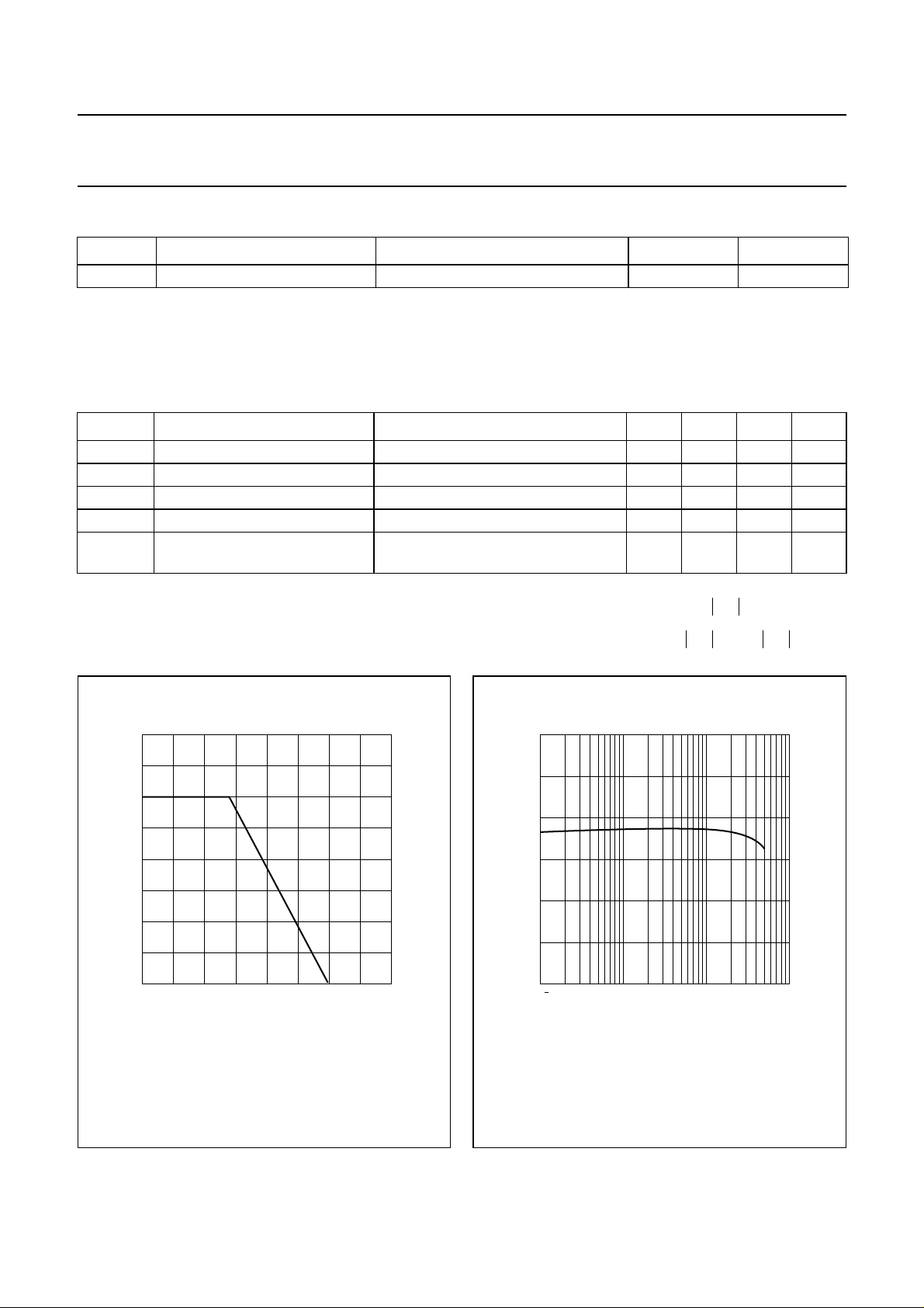
400
P
tot
(mW)
300
200
100
0
0 50 100 200
150
Ts (
MBB401
o
C)
140
handbook, halfpage
h
FE
100
60
20
1
2
S
G
UM
10 log
--------------------------------------------------------------
1S
–
110
21
2
1S
–
11
10
I (mA)
22
MBB397
C
10
dB=
2
2
Fig.2 Power derating curve.
September 1995 3
VCE=10V.
Fig.3 DC current gain as a function of collector
current.
Page 4
Philips Semiconductors Product specification
NPN 1 GHz wideband transistor BF547
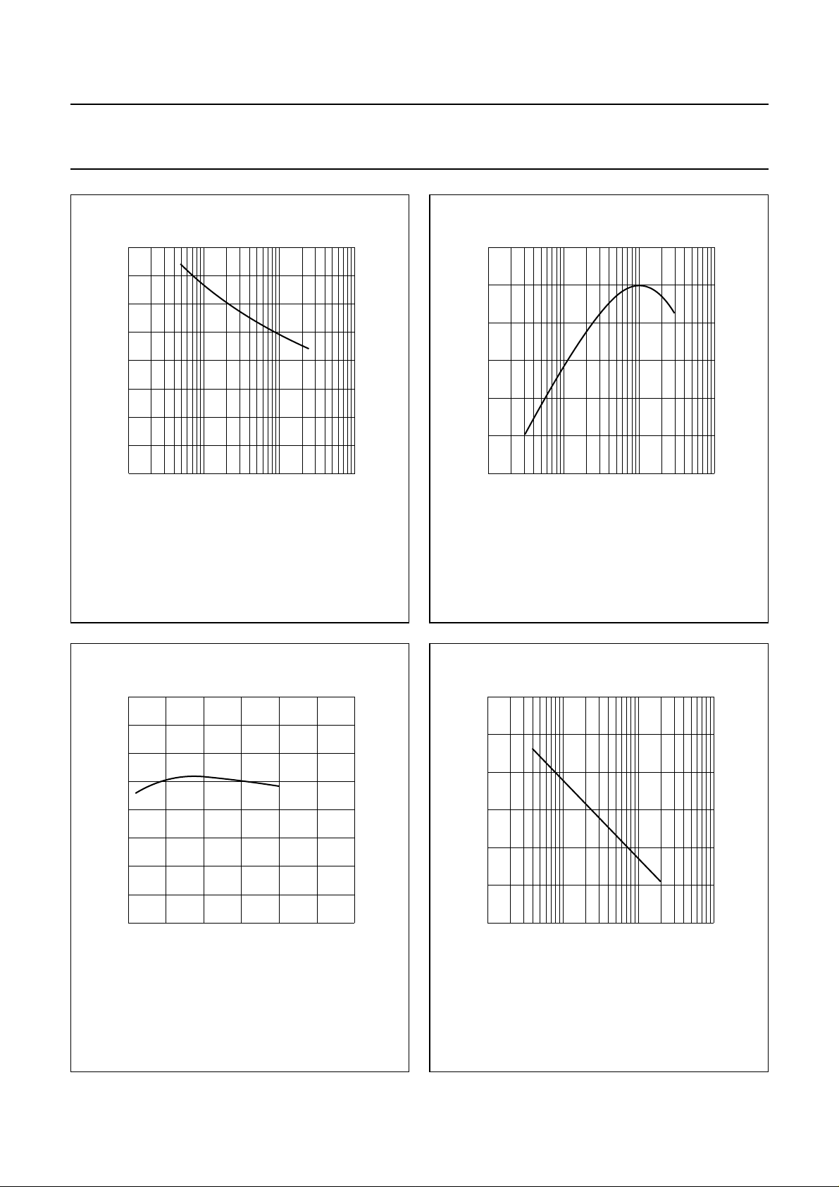
1.6
handbook, halfpage
C
re
(pF)
0.8
0
0.1
IE=ie= 0; f= 1 MHz.
1 10 100
VCB (V)
Fig.4 Feedback capacitance as a function of
collector-base voltage
MBB474
1.4
handbook, halfpage
f
T
(GHz)
1.0
0.6
0.2
−1
10
VCE= 10 V; f = 500 MHz.
110
IC (mA)
Fig.5 Transition frequency as a function of
collector current.
MBB399
2
10
40
handbook, halfpage
G
UM
(dB)
30
20
10
0
0102030
VCE= 10 V; f = 100 MHz.
IC (mA)
Fig.6 Maximum unilateral power gain as a
function of collector current.
MBB407
50
handbook, halfpage
G
UM
(dB)
40
30
20
10
0
−10
10
VCE= 10 V; IC=15mA.
2
10
3
10
f (MHz)
Fig.7 Maximum unilateral power gain as a
function of frequency.
MBB408
4
10
September 1995 4
Page 5

Philips Semiconductors Product specification
NPN 1 GHz wideband transistor BF547
10
handbook, halfpage
V
CE sat
(V)
1
−1
10
−2
10
−1
10
IC/IB= 10.
1
10
MBB398
IC (mA)
Fig.8 Collector-emitter saturation voltage as a
function of collector current.
IC (mA)
MBB409
2
handbook, halfpage
2
10
8
F
(dB)
6
4
2
0
−1
10
VCE= 10 V; ZS=ZL=50Ω; f = 100 MHz.
11010
Fig.9 Common emitter noise figure as a function
of collector current.
handbook, halfpage
0
b
f = 1000 MHz
11
(mS)
−20
−40
−60
−80
10 60
VCB=10V.
800
600
400
20 30 40 50
200
MBB410
IE = −2 mA
−5 mA
−10 mA
g11 (mS)
Fig.10 Common base input admittance (Y11).
September 1995 5
80
handbook, halfpage
b
21
(mS)
−5 mA
60
40
IE = −2 mA
200
20
0
−50 −40 −30 −20 −10
VCB=10V.
−10 mA
300
500
600
800
f = 1000 MHz
010
g21 (mS)
Fig.11 Common base forward admittance (Y21).
MBB413
Page 6

Philips Semiconductors Product specification
NPN 1 GHz wideband transistor BF547
handbook, halfpage
0
b
12
(mS)
−0.5
−1.0
−1.5
−2.0
−2.5
−0.7 −0.5 −0.3 −0.1
VCB=10V.
IE = −10 mA
−5 mA
f = 1000 MHz
−2 mA
300
500
600
800
g12 (mS)
Fig.12 Common base reverse admittance (Y12).
MBB411
200
handbook, halfpage
8
b
22
(mS)
6
4
2
0
0
VCB=10V.
200
I
E =
f = 1000 MHz
800
600
500
300
0.4 0.8 1.2 1.6
−2 mA
−5 mA
g22 (mS)
Fig.13 Common base output admittance (Y22).
MBB412
−10 mA
September 1995 6
Page 7

Philips Semiconductors Product specification
NPN 1 GHz wideband transistor BF547
handbook, full pagewidth
VCE= 10 V; IC= 15 mA; ZO=50Ω.
50
25
10
+ j
0
− j
10
10 25 50
25
3 GHz
100 250
50
100
40 MHz
100
Fig.14 Common emitter input reflection coefficient (S11).
250
∞
250
MBB403
handbook, full pagewidth
VCE= 10 V; IC=15mA.
o
90
120
40 MHz
o
150
20 16 8 4 2
o
180
o
150
120
o
3 GHz
o
o
90
o
60
o
30
o
0
o
30
o
60
MBB405
Fig.15 Common emitter forward transmission coefficient (S21).
+
− ϕ
ϕ
September 1995 7
Page 8

Philips Semiconductors Product specification
NPN 1 GHz wideband transistor BF547
o
handbook, full pagewidth
120
o
90
o
60
VCE= 10 V; IC=15mA.
handbook, full pagewidth
180
o
150
o
o
150
o
120
40 MHz
o
90
3 GHz
30
0.1 0.2 0.3 0.4 0.5
30
o
60
MBB406
o
o
0
o
Fig.16 Common emitter reverse transmission coefficient (S12).
50
25
100
+ ϕ
− ϕ
10
+ j
0
− j
10
VCE = 10 V; IC = 15 mA; ZO=50Ω.
10 25 50 100 250
25
Fig.17 Common emitter output reflection coefficient (S22).
September 1995 8
250
∞
40 MHz
250
3 GHz
100
50
MBB404
Page 9

Philips Semiconductors Product specification
NPN 1 GHz wideband transistor BF547
Table 1 Common base Y-parameters; VCB= 10 V; IE= −2mA
f (MHz)
REAL
(mS)
Y
11
IMAG.
(mS)
REAL
(mS)
Y
21
IMAG.
(mS)
REAL
(mS)
Y
12
IMAG.
(mS)
REAL
(mS)
Y
22
IMAG.
(mS)
40 69.0 −10.2 −68.0 12.3 −0.02 −0.1 −0.01 0.3
100 60.4 −20.6 −58.0 25.6 −0.06 −0.3 −0.08 0.7
200 45.0 −27.4 −39.1 34.5 −0.10 −0.6 0.19 1.4
300 34.3 −26.4 −25.4 34.0 −0.20 −0.8 0.29 1.9
400 27.7 −23.3 −17.2 31.1 −0.20 −1.0 0.37 2.5
500 24.0 −20.4 −11.7 27.6 −0.20 −1.2 0.45 3.0
600 21.5 −18.0 −7.8 25.0 −0.20 −1.4 0.53 3.6
700 20.0 −15.6 −5.3 22.6 −0.20 −1.6 0.60 4.2
800 18.6 −14.0 −3.0 20.2 −0.20 −1.8 0.69 4.7
900 18.3 −12.8 −1.3 18.7 −0.20 −2.0 0.82 5.3
1000 17.8 −11.7 −0.1 17.1 −0.20 −2.2 0.95 5.9
Table 2 Common base Y-parameters; V
Y
11
f (MHz)
REAL
(mS)
IMAG.
(mS)
= 10 V; IE= −5mA
CB
Y
21
REAL
(mS)
IMAG.
(mS)
REAL
(mS)
Y
12
IMAG.
(mS)
REAL
(mS)
Y
22
IMAG.
(mS)
40 132.6 −35.7 −130.5 38.8 −0.06 −0.2 −0.06 0.4
100 96.3 −62.0 −91.1 67.9 −0.20 −0.5 0.21 0.8
200 54.7 −57.8 −46.0 64.7 −0.30 −0.7 0.38 1.4
300 37.5 −46.9 −26.4 53.8 −0.40 −0.8 0.47 2.0
400 29.2 −38.6 −16.6 45.8 −0.40 −1.0 0.58 2.5
500 25.3 −32.8 −11.0 39.8 −0.40 −1.3 0.63 3.1
600 22.0 −28.4 −6.3 35.0 −0.40 −1.4 0.71 3.6
700 20.3 −25.2 −3.3 31.4 −0.40 −1.6 0.80 4.2
800 18.7 −22.6 −0.6 27.6 −0.40 −1.9 0.88 4.7
900 17.8 −20.7 1.4 25.2 −0.40 −2.1 1.01 5.3
1000 17.3 −19.1 3.0 23.0 −0.40 −2.3 1.15 6.0
September 1995 9
Page 10

Philips Semiconductors Product specification
NPN 1 GHz wideband transistor BF547
Table 3 Common base Y-parameters; VCB= 10 V; IE= −10 mA
f (MHz)
REAL
(mS)
Y
11
IMAG.
(mS)
REAL
(mS)
Y
21
IMAG.
(mS)
REAL
(mS)
Y
12
IMAG.
(mS)
REAL
(mS)
Y
22
IMAG.
(mS)
40 189.0 −79.6 −185.5 83.0 −0.10 −0.3 −0.09 0.4
100 108.5 −99.0 −101.4 105.4 −0.30 −0.5 0.30 0.9
200 55.2 −76.2 −44.6 82.8 −0.50 −0.7 0.44 1.4
300 37.1 −59.0 −24.3 65.7 −0.50 −0.9 0.60 2.0
400 28.8 −47.6 −14.6 54.4 −0.60 −1.0 0.69 2.5
500 24.7 −40.2 −8.6 46.7 −0.60 −1.3 0.75 3.1
600 21.2 −35.0 −3.4 40.8 −0.60 −1.5 0.84 3.6
700 19.3 −31.0 −0.2 36.2 −0.60 −1.7 0.93 4.2
800 17.2 −27.5 2.6 31.1 −0.60 −1.9 1.00 4.7
900 16.4 −25.2 4.6 28.3 −0.60 −2.1 1.15 5.3
1000 15.8 −23.0 6.0 25.5 −0.60 −2.3 1.31 6.0
Table 4 Common base Y-parameters; V
Y
11
f (MHz)
REAL
(mS)
IMAG.
(mS)
= 10 V; IE= −15 mA
CB
Y
21
REAL
(mS)
IMAG.
(mS)
REAL
(mS)
Y
12
IMAG.
(mS)
REAL
(mS)
Y
22
IMAG.
(mS)
40 206.5 −113.8 −202.6 118.1 −0.20 −0.3 0.2 0.5
100 104.3 −114.0 −96.4 120.1 −0.40 −0.5 0.4 0.9
200 53.1 −81.1 −41.7 87.7 −0.50 −0.7 0.6 1.4
300 35.9 −62.1 −22.0 68.6 −0.60 −0.8 0.7 2.0
400 28.1 −50.0 −12.5 56.9 −0.60 −1.1 0.8 2.5
500 23.4 −42.3 −6.1 48.2 −0.60 −1.3 0.8 3.1
600 20.1 −36.4 −1.2 41.6 −0.60 −1.5 0.9 3.6
700 18.2 −32.0 2.0 36.7 −0.60 −1.7 1.0 4.2
800 16.2 −28.2 4.5 31.3 −0.60 −1.9 1.1 4.7
900 15.5 −25.7 6.5 28.1 −0.60 −2.1 1.3 5.3
1000 14.7 −23.5 7.9 24.9 −0.60 −2.3 1.4 5.9
September 1995 10
Page 11

Philips Semiconductors Product specification
NPN 1 GHz wideband transistor BF547
PACKAGE OUTLINE
3.0
handbook, full pagewidth
0.55
0.45
0.150
0.090
2.8
1.9
0.95
21
B
A
M
A
0.2
30
max
0.1
max
max
o
2.5
1.4
max
M0.1 AB
1.2
MBC846
o
10
3
0.48
0.38
TOP VIEW
Dimensions in mm.
10
max
o
1.1
max
Fig.18 SOT23.
DEFINITIONS
Data sheet status
Objective specification This data sheet contains target or goal specifications for product development.
Preliminary specification This data sheet contains preliminary data; supplementary data may be published later.
Product specification This data sheet contains final product specifications.
Limiting values
Limiting values given are in accordance with the Absolute Maximum Rating System (IEC 134). Stress above one or
more of the limiting values may cause permanent damage to the device. These are stress ratings only and operation
of the device at these or at any other conditions above those given in the Characteristics sections of the specification
is not implied. Exposure to limiting values for extended periods may affect device reliability.
Application information
Where application information is given, it is advisory and does not form part of the specification.
LIFE SUPPORT APPLICATIONS
These products are not designed for use in life support appliances, devices, or systems where malfunction of these
products can reasonably be expected to result in personal injury. Philips customers using or selling these products for
use in such applications do so at their own risk and agree to fully indemnify Philips for any damages resulting from such
improper use or sale.
September 1995 11
 Loading...