

Page 1
DISCRETE SEMICONDUCTORS
DATA SH EET
BF545A; BF545B; BF545C
N-channel silicon junction
field-effect transistors
Product specification
Supersedes data of April 1995
File under Discrete Semiconductors, SC07
1996 Jul 29
Page 2
Philips Semiconductors Product specification
N-channel silicon junction
field-effect transistors
FEATURES
• Low leakage level (typ. 500 fA)
• High gain
• Low cut-off voltage (max. 2.2 V for BF545A).
APPLICATIONS
• Impedance converters in e.g. electret microphones and
infra-red detectors
• VHF amplifiers in oscillators and mixers.
DESCRIPTION
N-channel symmetrical silicon junction field-effect
transistors in a SOT23 package.
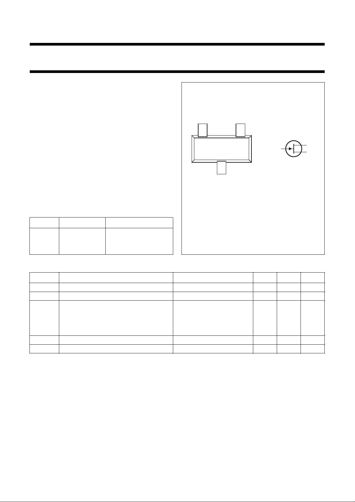
PINNING - SOT23
PIN SYMBOL DESCRIPTION
1 s source
2 d drain
3 g gate
handbook, halfpage
Marking codes:
BF545A: M65.
BF545B: M66.
BF545C: M67.
21
Top view
Fig.1 Simplified outline and symbol.
BF545A; BF545B; BF545C
d
s
3
g
MAM036
QUICK REFERENCE DATA
SYMBOL PARAMETER CONDITIONS MIN. MAX. UNIT
V
V
I
DSS
DS
GSoff
drain-source voltage −±30 V
gate-source cut-off voltage ID=1µA; VDS=15V −0.4 −7.8 V
drain current VGS= 0; VDS=15V
BF545A 2 6.5 mA
BF545B 6 15 mA
BF545C 12 25 mA
P
tot
y
forward transfer admittance VGS= 0; VDS= 15 V 3 6.5 mS
fs
total power dissipation up to T
=25°C − 250 mW
amb
1996 Jul 29 2
Page 3
Philips Semiconductors Product specification
N-channel silicon junction
BF545A; BF545B; BF545C
field-effect transistors
LIMITING VALUES
In accordance with the Absolute Maximum Rating System (IEC 134).
SYMBOL PARAMETER CONDITIONS MIN. MAX. UNIT
V
DS
V
GSO
V
GDO
I
G
P
tot
T
stg
T
j
Note
1. Device mounted on an FR4 printed-circuit board, maximum lead length 4 mm; mounting pad for the drain
lead 10 mm
handbook, halfpage
P
(mW)
drain-source voltage −±30 V
gate-source voltage open drain −−30 V
gate-drain voltage (DC) open source −−30 V
forward gate current (DC) − 10 mA
total power dissipation up to T
=25°C; note 1 − 250 mW
amb
storage temperature −65 150 °C
operating junction temperature − 150 °C
2
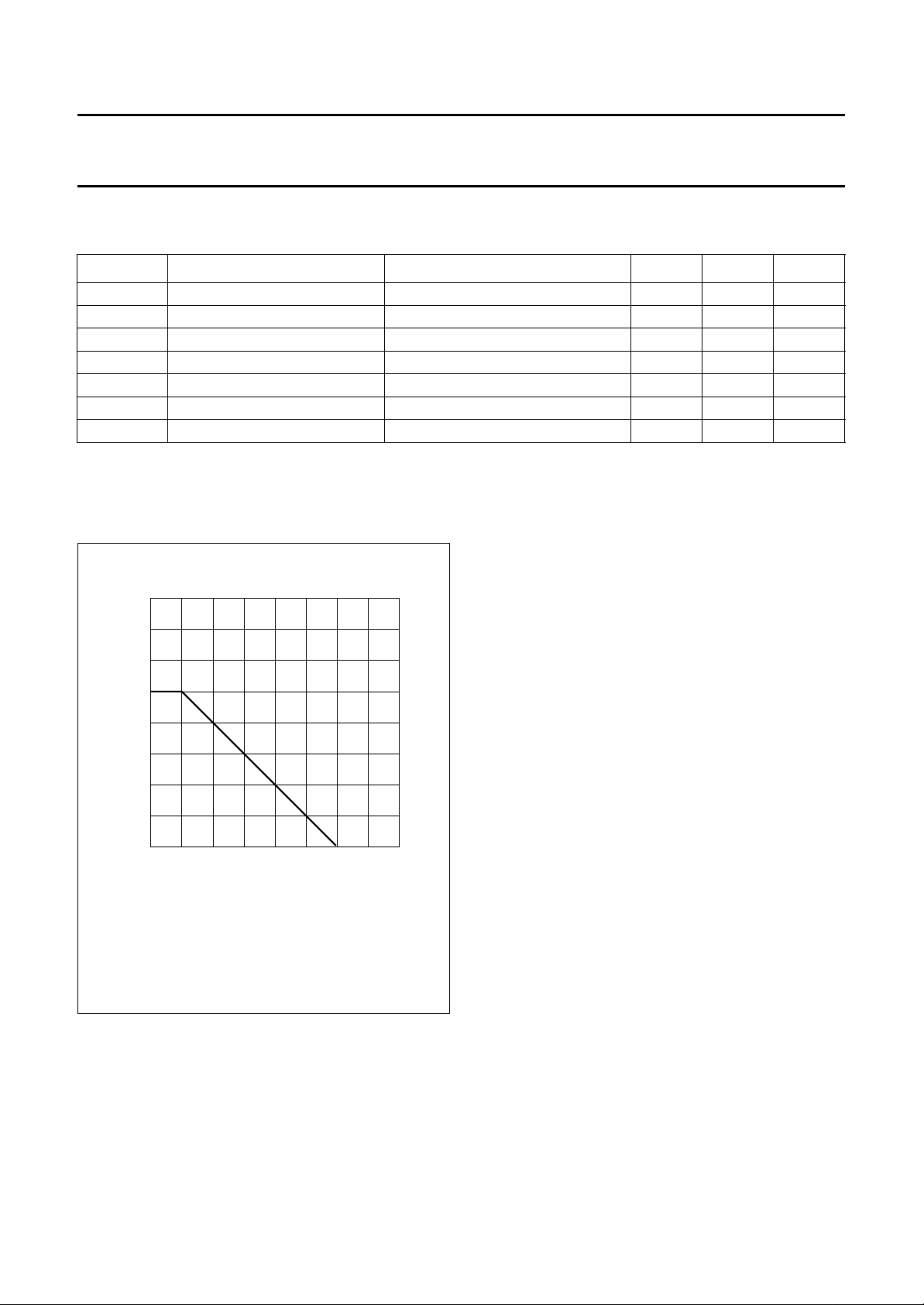
.
400
tot
300
MBB688
200
100
0
0 50 100 200
150
T
amb
Fig.2 Power derating curve.
(°C)
1996 Jul 29 3
Page 4

Philips Semiconductors Product specification
N-channel silicon junction
BF545A; BF545B; BF545C
field-effect transistors
THERMAL CHARACTERISTICS
SYMBOL PARAMETER VALUE UNIT
R
th j-a
Note
1. Device mounted on an FR4 printed-circuit board, maximum lead length 4 mm; mounting pad for the drain
lead 10 mm
STATIC CHARACTERISTICS
=25°C; unless otherwise specified.
T
j
SYMBOL PARAMETER CONDITIONS MIN. TYP. MAX. UNIT
V
(BR)GSS
V
GSoff
I
DSS
I
GSS
forward transfer admittance VGS= 0; VDS=15V 3 − 6.5 mS
y
fs
common source output
y
os
thermal resistance from junction to ambient; note 1 500 K/W
2
.
gate-source breakdown voltage IG= −1 µA; VDS=0 −30 −−V
gate-source cut-off voltage ID= 200 µA; VDS=15V
BF545A −0.4 −−2.2 V
BF545B −1.6 −−3.8 V
BF545C −3.2 −−7.8 V
=1µA; VDS=15V −0.4 −−7.5 V
I
D
drain current VGS= 0; VDS=15V
BF545A 2 − 6.5 mA
BF545B 6 − 15 mA
BF545C 12 − 25 mA
gate leakage current VGS= −20 V; VDS=0 −−0.5 −1000 pA
= −20 V; VDS=0;
V
GS
−−−100 nA
Tj= 125 °C
VGS= 0; VDS=15V − 40 −µS
admittance
1996 Jul 29 4
Page 5

Philips Semiconductors Product specification
N-channel silicon junction
BF545A; BF545B; BF545C
field-effect transistors
DYNAMIC CHARACTERISTICS
T
=25°C; unless otherwise specified.
amb
SYMBOL PARAMETER CONDITIONS TYP. UNIT
C
is
C
rs
g
is
g
fs
g
rs
g
os
input capacitance VDS=15V; VGS= −10 V; f = 1 MHz 1.7 pF
=15V; VGS= 0; f = 1 MHz 3 pF
V
DS
reverse transfer capacitance VDS=15V; VGS= −10 V; f = 1 MHz 0.8 pF
=15V; VGS= 0; f = 1 MHz 0.9 pF
V
DS
common source input conductance VDS=10V; ID= 1 mA; f = 100 MHz 15 µS
=10V; ID= 1 mA; f = 450 MHz 300 µS
V
DS
common source transfer
conductance
common source reverse
conductance
common source output
conductance
VDS=10V; ID= 1 mA; f = 100 MHz 2 mS
=10V; ID= 1 mA; f = 450 MHz 1.8 mS
V
DS
VDS=10V; ID= 1 mA; f = 100 MHz −6 µS
=10V; ID= 1 mA; f = 450 MHz −40 µS
V
DS
VDS=10V; ID= 1 mA; f = 100 MHz 30 µS
=10V; ID= 1 mA; f = 450 MHz 60 µS
V
DS
30
handbook, halfpage
I
DSS
(mA)
20
10
0
0
VDS= 15V; Tj=25°C.
−2
−4 −8
MBB467
−6
V
GSoff
Fig.3 Drain current as a function of gate-source
cut-off voltage; typical values.
(V)
handbook, halfpage
6
Y
fs
(mS)
5
4
0
VDS= 15V; VGS= 0; Tj=25°C.
−2
−4 −8
Fig.4 Forward transfer admittance as a
function of gate-source cut-off voltage;
typical values.
MBB466
−6
V
(V)
GSoff
1996 Jul 29 5
Page 6

Philips Semiconductors Product specification
N-channel silicon junction
field-effect transistors
80
handbook, halfpage
Y
os
(µS)
40
0
0
VDS= 15V; VGS= 0; Tj=25°C.
−2
−4 −8−6
V
GSoff
MBB465
(V)
BF545A; BF545B; BF545C
300
handbook, halfpage
R
DSon
(Ω)
200
100
0
0
VDS= 100mV; VGS= 0; Tj=25°C.
−2
MBB464
−4 −8
−6
V
(V)
GSoff
Fig.5 Common-source output admittance as a
function of gate-source cut-off voltage;
typical values.
MBB462
V
GS
−0.5 V
−1.0 V
VDS (V)
= 0 V
I
D
(mA)
6
4
2
0
0
handbook, halfpage
Fig.6 Drain-source on-resistance as a
function of gate-source cut-off voltage;
typical values.
handbook, halfpage
164812
6
I
D
(mA)
4
2
0
−3 −2 −10
MBB463
VGS (V)
Tj=25°C.
Fig.7 Typical output characteristics; BF545A.
1996 Jul 29 6
VDS= 15V; Tj=25°C.
Fig.8 Typical input characteristics; BF545A.
Page 7

Philips Semiconductors Product specification
N-channel silicon junction
field-effect transistors
16
handbook, halfpage
I
D
(mA)
12
8
4
0
0
MBB460
VGS = 0 V
−0.5 V
−1 V
−1.5 V
−2 V
−2.5 V
VDS (V)
BF545A; BF545B; BF545C
16
handbook, halfpage
I
D
(mA)
12
8
4
0
164812
−6 −4 −20
MBB459
VGS (V)
Tj=25°C.
Fig.9 Typical output characteristics; BF545B.
30
handbook, halfpage
I
D
(mA)
20
10
0
0
VGS = 0 V
VDS (V)
MBB457
−1 V
−2 V
−3 V
−4 V
−5 V
VDS= 15V; Tj=25°C.
Fig.10 Typical input characteristics; BF545B.
30
handbook, halfpage
I
D
(mA)
20
10
0
164812
−8 −6 −4 −20
MBB456
VGS (V)
Tj=25°C.
Fig.11 Typical output characteristics; BF545C.
1996 Jul 29 7
VDS= 15V; Tj=25°C.
Fig.12 Typical input characteristics; BF545C.
Page 8

Philips Semiconductors Product specification
N-channel silicon junction
field-effect transistors
3
10
handbook, halfpage
ID
(µA)
2
10
10
1
−1
10
−2
10
−3
10
BF545A; BF545B; BF545C
MBB461
handbook, halfpage
(V)
0−3 −2 −1
V
GS
ID
(µA)
3
10
2
10
10
1
−1
10
−2
10
−3
10
MBB458
(V)
0−6 −4 −2
V
GS
VDS= 15V; Tj=25°C.
Fig.13 Drain current as a function of gate-source
voltage; typical values for BF545A.
V
GS
MBB455
(V)
3
10
handbook, halfpage
ID
(µA)
2
10
10
1
−1
10
−2
10
−3
10
VDS= 15V; Tj=25°C.
Fig.14 Drain current as a function of gate-source
voltage; typical values for BF545B.
1 mA
0.1 mA
VDG (V)
MBB454
20100
2
−10
handbook, halfpage
I
G
(pA)
−10
−1
I
GSS
−1
−10
−2
0−8 −6 −4 −2
−10
ID = 10 mA
VDS= 15V; Tj=25°C.
Fig.15 Drain current as a function of gate-source
voltage; typical values for BF545C.
1996 Jul 29 8
ID= 10mA only for BF545B and BF545C; Tj=25°C.
Fig.16 Gate current as a function of drain-gate
voltage; typical values.
Page 9

Philips Semiconductors Product specification
N-channel silicon junction
field-effect transistors
3
−10
handbook, halfpage
I
GSS
(pA)
2
−10
−10
−1
−1
−10
−50 0 50 100 150
MBB453
Tj (°C)
handbook, halfpage
1
C
rs
(pF)
0.5
0
−10 −50
BF545A; BF545B; BF545C
MBB452
VGS (V)
VDS= 0; VGS= −20V.
Fig.17 Gate current as a function of junction
temperature; typical values.
handbook, halfpage
3
C
is
(pF)
2
1
0
−10 −50
VGS (V)
MBB451
VDS= 15V; Tj=25°C.
Fig.18 Reverse transfer capacitance as a function
of gate-source voltage; typical values.
2
10
handbook, halfpage
y
is
(mS)
10
1
−1
10
−2
10
10
b
is
g
is
2
10
MBB468
f (MHz)
3
10
VDS= 15V; Tj=25°C.
Fig.19 Typical input capacitance.
1996 Jul 29 9
VDS= 10V; ID= 1mA; T
amb
=25°C.
Fig.20 Common-source input admittance;
typical values.
Page 10

Philips Semiconductors Product specification
N-channel silicon junction
field-effect transistors
2
10
handbook, halfpage
Y
fs
(mS)
10
g
fs
1
–b
fs
–1
10
10
2
10
f (MHz)
MBB469
BF545A; BF545B; BF545C
f (MHz)
MBB470
3
10
10
handbook, halfpage
y
rs
(mS)
1
−1
10
−2
10
−3
3
10
10
10 10
−brs
−grs
2
VDS= 10V; ID= 1mA; T
amb
=25°C.
Fig.21 Common-source forward transfer
admittance; typical values.
10
handbook, halfpage
y
os
(mS)
1
−1
10
−2
10
10 10
bos
gos
2
f (MHz)
MBB471
VDS= 10V; ID= 1mA; T
amb
=25°C.
Fig.22 Common-source reverse transfer
admittance; typical values.
3
10
VDS= 10V; ID= 1mA; T
amb
=25°C.
Fig.23 Common-source output admittance;
typical values.
1996 Jul 29 10
Page 11

Philips Semiconductors Product specification
N-channel silicon junction
field-effect transistors
PACKAGE OUTLINE
handbook, full pagewidth
0.55
0.45
o
10
max
1.1
max
30
max
0.150
0.090
0.1
max
max
o
BF545A; BF545B; BF545C
3.0
2.8
1.9
0.95
21
o
10
3
0.48
0.38
TOP VIEW
A
M0.1 AB
B
1.4
1.2
2.5
max
MBC846
0.2
A
M
Dimensions in mm.
Fig.24 SOT23.
1996 Jul 29 11
Page 12

Philips Semiconductors Product specification
N-channel silicon junction
BF545A; BF545B; BF545C
field-effect transistors
DEFINITIONS
Data Sheet Status
Objective specification This data sheet contains target or goal specifications for product development.
Preliminary specification This data sheet contains preliminary data; supplementary data may be published later.
Product specification This data sheet contains final product specifications.
Limiting values
Limiting values given are in accordance with the Absolute Maximum Rating System (IEC 134). Stress above one or
more of the limiting values may cause permanent damage to the device. These are stress ratings only and operation
of the device at these or at any other conditions above those given in the Characteristics sections of the specification
is not implied. Exposure to limiting values for extended periods may affect device reliability.
Application information
Where application information is given, it is advisory and does not form part of the specification.
LIFE SUPPORT APPLICATIONS
These products are not designed for use in life support appliances, devices, or systems where malfunction of these
products can reasonably be expected to result in personal injury. Philips customers using or selling these products for
use in such applications do so at their own risk and agree to fully indemnify Philips for any damages resulting from such
improper use or sale.
1996 Jul 29 12
 Loading...