

Page 1
®
SMALL S IGNAL PNP TRANSISTOR
Ordering Code Marking Package / Shipment
BF421 BF421 TO-92 / Bulk
BF421-AP BF421 TO-92 / Ammopack
■ SILICON EPI TAX IA L PLANAR PN P HIGH
VOLTAGE TRANSISTOR
■ TO-92 PACKAGE SUITABLE FOR
THROU GH-HOLE PC B ASSEMBLY
■ THE NPN COMPL E ME NT ARY TYPE IS
BF420
APPLICATIONS
■ VIDEO AMPLIFIE R CIRCUI T S (RGB
CATHODE CURRENT CONTROL)
■ TELEPHONE WIRELINE INTERFACE (HOOK
SWITCHES, DIALER CIRCUITS)
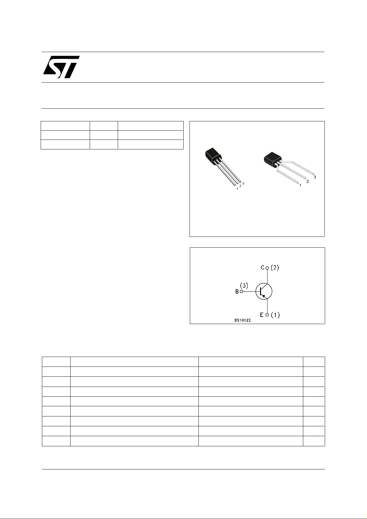
TO-92
Bulk
BF421
PRELIMINARY DATA
TO-92
Ammopack
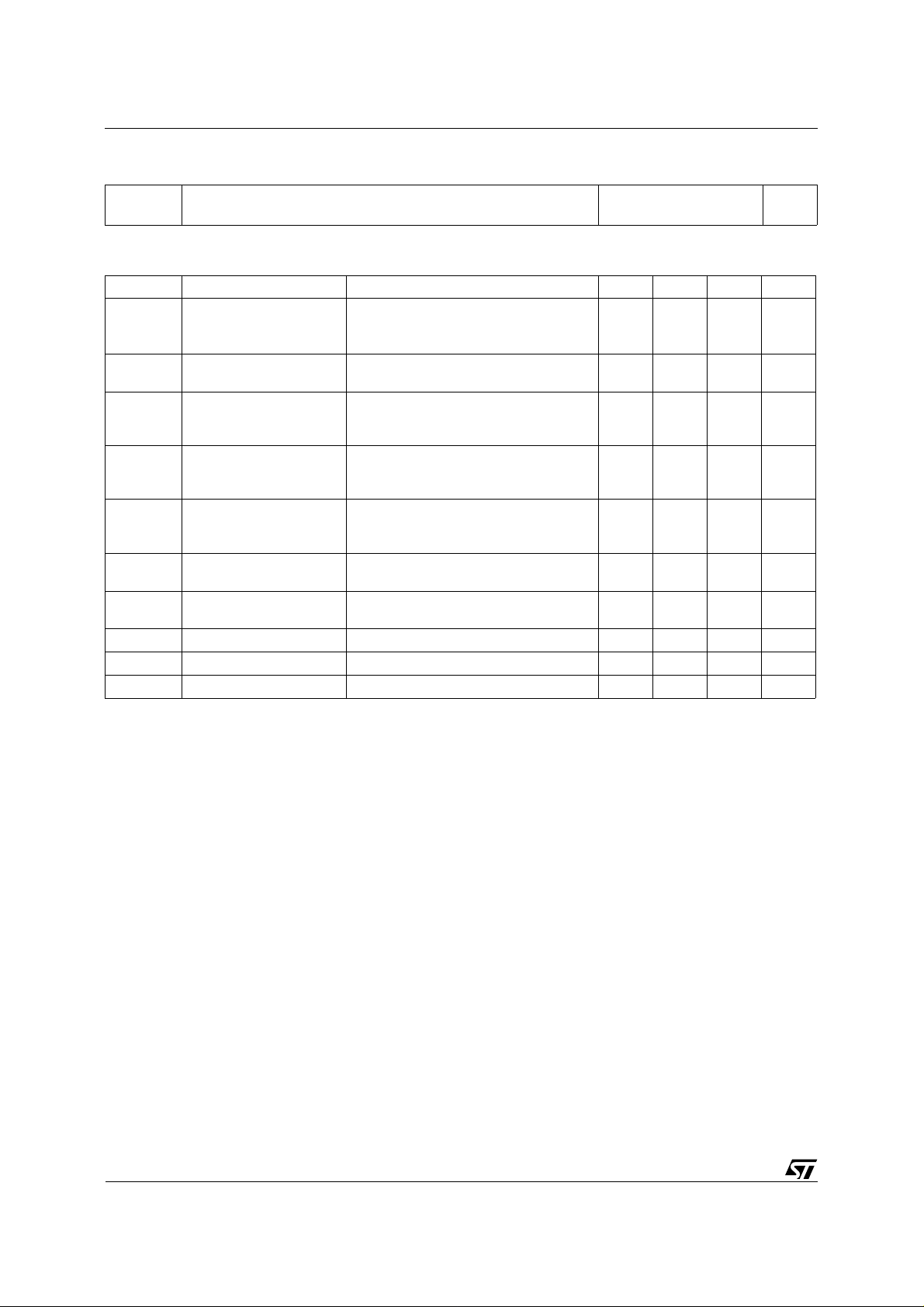
INTERNAL SCHEMATIC DIAGRAM
ABSOL UT E MAXIMU M RATINGS
Symbol Parameter Value Unit
V
V
V
I
P
T
Collector-Base Voltage (IE = 0) -300 V
CBO
Collector-Emitter Voltage (IB = 0) -300 V
CEO
Emitter-Base Voltage (IC = 0) -5 V
EBO
I
Collector Current -500 mA
C
Collector Peak Current (tp < 5ms) -600 mA
CM
Total Dissipation at TC = 25 oC 830 mW
tot
Storage Temperature -65 to 150
stg
T
Max. Operating Junction Temperature 150
j
o
C
o
C
February 2003
1/5
Page 2
BF421
THERMAL DATA
R
R
thj-amb
thj-Case
•
Thermal Resistance Junction-Ambient Max
•
Thermal Resistance Junction-Case Max
150
50
o
C/W
o
C/W
ELECTRICAL CHARACTERISTICS (T
= 25 oC unless otherwise specified)
case
Symbol Parameter Test Conditions Min. Typ. Max. Unit
I
CBO
I
EBO
V
(BR)CEO
Collector Cut-off
Current (I
= 0)
E
Emitter Cut-off Current
(I
= 0)
C
∗ Collector-Emitter
= -200 V
V
CB
V
= -200 V TC = 150 oC
CB
V
= -300 V
CB
= -5 V -50 nA
V
EB
I
= -10 mA -300 V
C
-10
-10
-100
Breakdown Voltage
(I
= 0)
B
V
(BR)CBO
Collector-Base
= -10 µA
I
C
-300 V
Breakdown Voltage
(I
= 0)
E
V
(BR)EBO
Emitter-Base
= -100 µA
I
E
-5 V
Breakdown Voltage
(I
= 0)
C
V
CE(sat)
∗ Collector-Emitter
IC = -30 mA IB = -5 mA -0.6 V
Saturation Voltage
V
BE(sat)
∗ Base-Emitter
IC = -30 mA IB = -5 mA -1.2 V
Saturation Voltage
∗ DC Current Gain IC = -25 mA VCE = -20 V 50
h
FE
f
C
Transition Frequency IC = -10 mA VCE = -10 V f =100MHz 60 MHz
T
Reverse Capacitance IE = 0 VCB = -30 V f = 1MHz 1.6 pF
RE
∗ Pulsed: Pulse duration ≤ 300 µs, duty cycle ≤ 2 %
nA
µA
µA
2/5
Page 3

TO-92 MECHANICA L DAT A
BF421
DIM.
MIN. TYP. MAX. MIN. TYP. MAX.
A 4.32 4.95 0.170 0.195
b 0.36 0.51 0.014 0.020
D 4.45 4.95 0.175 0.194
E 3.30 3.94 0.130 0.155
e 2.41 2.67 0.095 0.105
e1 1.14 1.40 0.045 0.055
L 12.70 15.49 0.500 0.609
R 2.16 2.41 0.085 0.094
S1 1.14 1.52 0.045 0.059
W 0.41 0.56 0.016 0.022
V 4 degree 6 degree 4 degree 6 degree
mm inch
3/5
Page 4

BF421
TO-92 AMMOPACK SHIPMENT (Suffix"-AP") MECHANICAL DATA
DIM.
A1 4.80 0.189
T 3.80 0.150
T1 1.60 0.063
T2 2.30 0.091
d 0.48 0.019
P0 12.50 12.70 12.90 0.492 0.500 0.508
P2 5.65 6.35 7.05 0.222 0.250 0.278
F1,F2 2.44 2.54 2.94 0.096 0.100 0.116
delta H -2.00 2.00 -0.079 0.079
W 17.50 18.00 19.00 0.689 0.709 0.748
W0 5.70 6.00 6.30 0.224 0.236 0.248
W1 8.50 9.00 9.25 0.335 0.354 0.364
W2 0.50 0.020
H 18.50 20.50 0.728 0.807
H0 15.50 16.00 16.50 0.610 0.630 0.650
H1 25.00 0.984
D0 3.80 4.00 4.20 0.150 0.157 0.165
t 0.90 0.035
L 11.00 0.433
I1 3.00 0.118
delta P -1.00 1.00 -0.039 0.039
MIN. TYP. MAX. MIN. TYP. MAX.
mm inch
4/5
Page 5

BF421
Information furnished is believed to be accurate and reliable. However, STMicroelectronics assumes no responsibility for the consequences
of use of such inform ation nor for any infringe ment o f patents or other rig hts o f third par ties which ma y resul t from i ts use. N o li cen se is
granted by implicatio n or otherwise under any patent or patent rights of STMicroelectronics. Specification mentioned in this publication are
subject to change without notice. This publication supersedes and replaces all information previously supplied. STMicroelectronics products
are not authorized for use as critical compo nents in life support devices or systems without express written approval of STMicroelectronics.
The ST logo is a trademark of STMicroelectronics
© 2003 STMicroelectro nics – Printed in Italy – All Rights Reserved
STMicroelectronics GROUP OF COMPANIES
Australia - Brazil - Canada - China - Finland - France - Germany - Hong Kong - India - Israel - Italy - Japan - Malaysia - Malta - Morocco -
Singapore - Spain - Sweden - Switzerland - United Kingdom - United States.
http://www.st.com
5/5
 Loading...