

Page 1

BDX53B / BDX53C
COMPLEMENTARY SILICON POWER
■ STMicroelectronicsPREFERRED
SALESTYPES
APPLICATIONS
■ AUDIO AMPLIFIERS
■ LINEARAND SWITCHING INDUSTRIAL
EQUIPMENT
DESCRIPTION
The BDX53B and BDX53C are silicon
Epitaxial-Base NPN power transistors in
monolithic Darlington configuration mounted in
Jedec TO-220 plastic package. They are intented
for use in hammer drivers, audio amplifiers and
other medium power linear and switching
applications.
The complementary PNP types are BDX54B and
BDX54Crespectively.
BDX54B / BDX54C
DARLINGTONTRANSISTORS
3
2
1
TO-220
INTERNAL SCHEMATIC DIAGRAM
R1Typ. = 10 KΩ R2Typ. = 150 Ω
ABSOLUTE MAXIMUM RATINGS
Symbol Parameter Value Unit
NPN BDX53 B BDX 53C
PNP BDX54B BDX54C
V
V
V
I
P
T
For PNP types voltage and current values are negative.
September 1999
Coll ect o r -B a s e V o lt age (IE= 0) 80 100 V
CBO
Coll ect o r -E mitt er Voltage ( IB= 0) 80 100 V
CEO
Emitter -base V o lt age (IC=0) 5 V
EBO
Coll ect o r Curr e nt 8 A
I
C
Collector Peak Current (repetitive) 12 A
CM
Base Current 0.2 A
I
B
Total Dissipation at Tc≤ 25 oC
tot
St orage Tempe rature -65 to 15 0
stg
Max. Operating Junction Temperature 150
T
j
60 W
o
C
o
C
1/6
Page 2
BDX53B - BDX53C - BDX54B - BDX54C
THERMAL DATA
R
thj-case
R
thj-amb
Ther mal Resist ance Junction-cas e Max
Ther mal Resist ance Junction-ambient Max
2.08
70
o
C/W
o
C/W
ELECTRICAL CHARACTERISTICS
=25oC unless otherwisespecified)
(T
case
Symbol Parameter Test Conditions Min. Typ. Max. Unit
I
CBO
I
CEO
I
EBO
V
CEO(sus )
V
CE(sat)
Collec to r Cut-of f
Current ( I
E
=0)
Collec to r Cut-of f
Current ( I
B
=0)
Emitter C ut-off Current
=0)
(I
C
∗ Collector-Emitter
Sust aining Voltage
=0)
(I
B
∗ Collector-e mit ter
for BDX53B/54B V
for BDX53C/54C V
for BDX53B/54B V
for BDX53C/54C V
V
=5V 2 mA
EB
I
=100mA forBDX5 3B/54B
C
for
=80V
CB
=100V
CB
=40V
CE
=50V
CE
BDX53 C/ 5 4C
80
100
0.2
0.2
0.5
0.5
IC=3A IB=12 mA 2 V
Sat uration Volt age
V
BE(sat)
∗ Base-emitter
IC=3A IB=12 mA 2.5 V
Sat uration Volt age
h
FE
V
DC Curre nt Gai n I
∗
∗ Parallel-diod e For wa r d
F
Voltage
∗
Pulsed: Pulse duration = 300µs, duty cycle 1.5 %
For PNP types voltage and current values are negative.
=3A VCE= 3 V 750
C
IF=3A
I
=8A
F
1.8
2.5
2.5 V
mA
mA
mA
mA
V
V
V
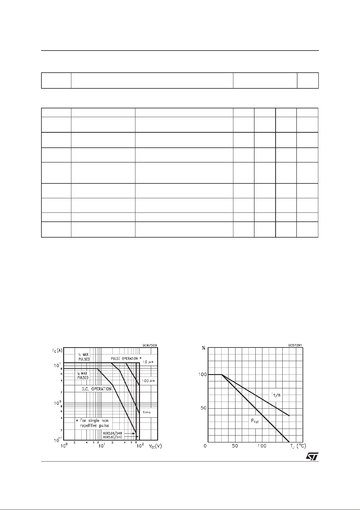
SafeOperating Area DeratingCurve
2/6
Page 3

BDX53B - BDX53C - BDX54B - BDX54C
DC CurrentGain (NPNtype)
CollectorEmitter Saturation Voltage(NPN type)
DC CurrentGain (PNP type)
CollectorEmitter Saturation Voltage(PNP type)
BaseEmitter Saturation Voltage(NPN type)
BaseEmitter Saturation Voltage(PNP type)
3/6
Page 4

BDX53B - BDX53C - BDX54B - BDX54C
BaseEmitter On Voltage(NPN type)
FreewheelDiode Forward Voltage (NPN type)
Base Emitter On Voltage(PNP type)
FreewheelDiode Forward Voltage (PNP type)
SwitchingTime Resistive Load (NPN type) SwitchingTime resistive Load (PNP type)
4/6
Page 5

BDX53B - BDX53C - BDX54B - BDX54C
TO-220 MECHANICAL DATA
DIM.
MIN. TYP. MAX. MIN. TYP. MAX.
A 4.40 4.60 0.173 0.181
C 1.23 1.32 0.048 0.051
D 2.40 2.72 0.094 0.107
D1 1.27 0.050
E 0.49 0.70 0.019 0.027
F 0.61 0.88 0.024 0.034
F1 1.14 1.70 0.044 0.067
F2 1.14 1.70 0.044 0.067
G 4.95 5.15 0.194 0.203
G1 2.4 2.7 0.094 0.106
H2 10.0 10.40 0.393 0.409
L2 16.4 0.645
L4 13.0 14.0 0.511 0.551
L5 2.65 2.95 0.104 0.116
L6 15.25 15.75 0.600 0.620
L7 6.2 6.6 0.244 0.260
L9 3.5 3.93 0.137 0.154
DIA. 3.75 3.85 0.147 0.151
mm inch
P011C
5/6
Page 6

BDX53B - BDX53C - BDX54B - BDX54C
Information furnished is believed to be accurate and reliable. However, STMicroelectronics assumes no responsibility for the consequences
of use of such information nor for any infringement of patents or other rights of third parties which may result from its use. No license is
granted by implication or otherwise under any patent or patent rights of STMicroelectronics. Specification mentioned in this publication are
subject to change without notice. This publication supersedes and replaces all information previously supplied. STMicroelectronics products
are not authorized foruse as critical components inlife support devices or systems without express written approval of STMicroelectronics.
The ST logo is a trademarkof STMicroelectronics
1999 STMicroelectronics – Printed in Italy – All Rights Reserved
STMicroelectronics GROUP OF COMPANIES
Australia - Brazil - China - Finland - France - Germany - Hong Kong - India - Italy - Japan - Malaysia - Malta - Morocco -
Singapore -Spain - Sweden - Switzerland - United Kingdom - U.S.A.
http://www.st.com
.
6/6
 Loading...