

Page 1
Î
Î
Î
Î
ON Semiconductor
NPN
Plastic High Power Silicon
Transistor
. . . designed for use in high power audio amplifiers utilizing
complementary or quasi complementary circuits.
• DC Current Gain —
hFE = 30 (Min) @ IC = 2.0 Adc
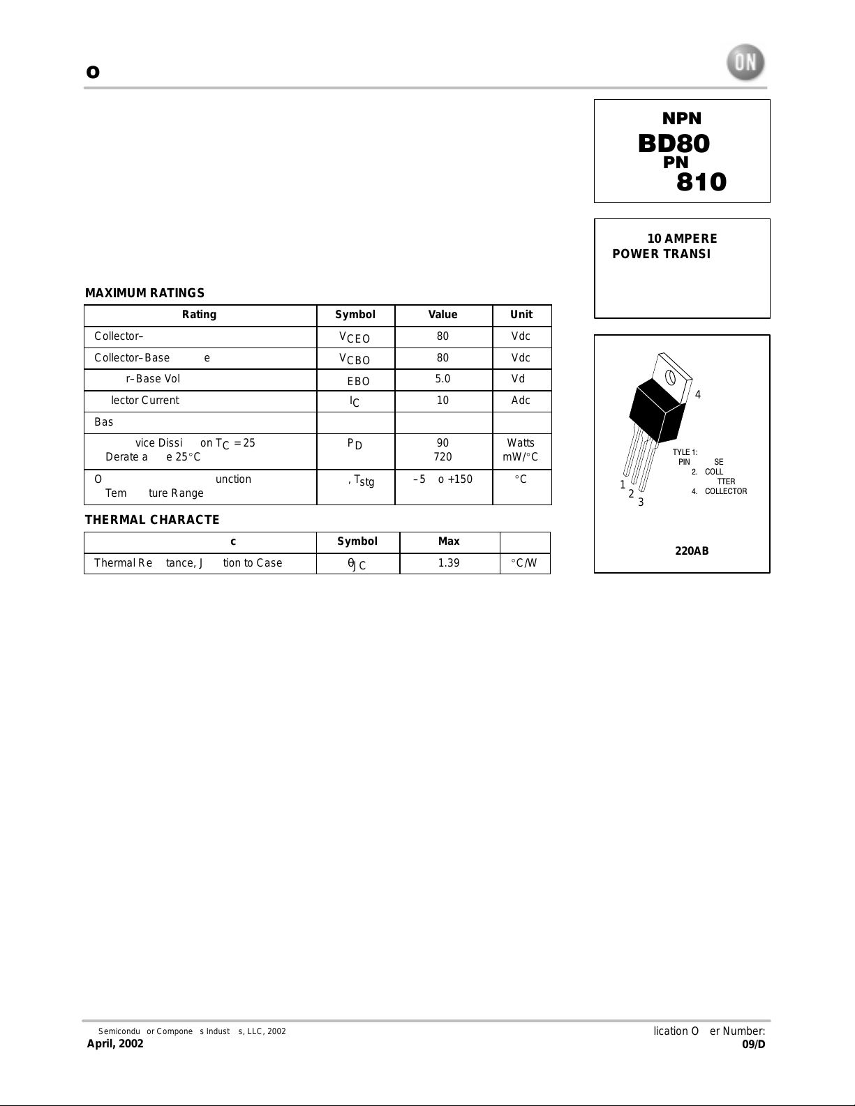
MAXIMUM RATINGS
Rating
Collector–Emitter Voltage
Collector–Base Voltage
Emitter–Base Voltage
Collector Current
Base Current
Total Device Dissipation TC = 25C
Derate above 25C
Operating and Storage Junction
ОООООООООО
Temperature Range
THERMAL CHARACTERISTICS
Characteristic
Thermal Resistance, Junction to Case
Symbol
V
CEO
V
CBO
V
EBO
I
C
I
B
P
D
TJ, T
stg
ÎÎÎ
Symbol
θ
JC
Value
5.0
6.0
720
–55 to +150
ÎÎÎ
80
80
10
90
Max
1.39
Unit
Vdc
Vdc
Vdc
Adc
Adc
Watts
mW/C
C
ÎÎ
Unit
C/W
BD809
PNP
BD810
10 AMPERE
POWER TRANSISTORS
PNP SILICON
60, 80 VOL TS
90 WATTS
4
STYLE 1:
PIN 1. BASE
2. COLLECTOR
1
2
3
CASE 221A–09
3. EMITTER
4. COLLECTOR
TO–220AB
Semiconductor Components Industries, LLC, 2002
April, 2002 – Rev. 1
1 Publication Order Number:
BD809/D
Page 2
BD809 BD810
ÎÎÎÎ
Î
Î
ÎÎÎÎ
Î
Î
Î
Î
Î
Î
ÎÎÎÎ
Î
Î
Î
Î
ÎÎÎÎ
Î
Î
Î
Î
ÎÎÎÎ
Î
Î
Î
Î
Î
Î
Î
Î
Î
Î
ÎÎÎÎ
Î
Î
Î
Î
ÎÎÎÎ
Î
Î
ÎÎÎÎ
Î
Î
Î
Î
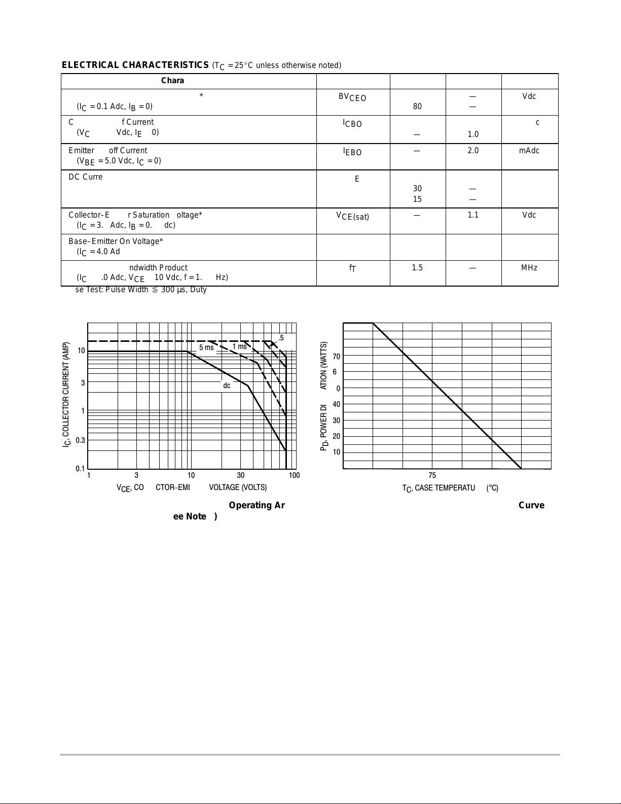
ELECTRICAL CHARACTERISTICS (T
= 25C unless otherwise noted)
C
Characteristic
Collector–Emitter Sustaining Voltage*
ОООООООООООООООО
(IC = 0.1 Adc, IB = 0)
Collector Cutoff Current
(VCB = 80 Vdc, IE = 0)
ОООООООООООООООО
Emitter Cutoff Current
(VBE = 5.0 Vdc, IC = 0)
DC Current Gain
ОООООООООООООООО
(IC = 2.0 A, VCE = 2.0 V)
(IC = 4.0 A, VCE = 2.0 V)
ОООООООООООООООО
Collector–Emitter Saturation Voltage*
(IC = 3.0 Adc, IB = 0.3 Adc)
ОООООООООООООООО
Base–Emitter On Voltage*
(IC = 4.0 Adc, VCE = 2.0 Vdc)
Current–Gain Bandwidth Product
ОООООООООООООООО
(IC = 1.0 Adc, VCE = 10 Vdc, f = 1.0 MHz)
*Pulse Test: Pulse Width 300 µs, Duty Cycle 2.0%.
.5 ms
10
5 ms
3
1 ms
dc
1 ms
1
, COLLECTOR CURRENT (AMP)
0.3
C
I
0.1
1
3 10 30 100
VCE, COLLECTOR-EMITTER VOLTAGE (VOLTS)
Figure 1. Active Region DC Safe Operating Area
(see Note 1)
Symbol
BV
CEO
ÎÎÎÎ
I
CBO
ÎÎÎÎ
I
EBO
h
FE
ÎÎÎÎ
ÎÎÎÎ
V
CE(sat)
ÎÎÎÎ
V
BE(on)
f
T
ÎÎÎÎ
Min
ÎÎ
80
—
ÎÎ
—
ÎÎ
30
15
ÎÎ
—
ÎÎ
—
1.5
ÎÎ
Max
—
ÎÎÎ
—
1.0
ÎÎÎ
2.0
ÎÎÎ
—
—
ÎÎÎ
1.1
ÎÎÎ
1.6
—
ÎÎÎ
ÎÎ
ÎÎ
ÎÎ
ÎÎ
ÎÎ
ÎÎ
90
80
70
60
50
40
30
20
, POWER DISSIPATION (WATTS)
D
P
10
0
0 25 50 100 125 150 175
75
T
, CASE TEMPERATURE (°C)
C
Figure 2. Power–Temperature Derating Curve
Unit
Vdc
mAdc
mAdc
Vdc
Vdc
MHz
http://onsemi.com
2
Page 3
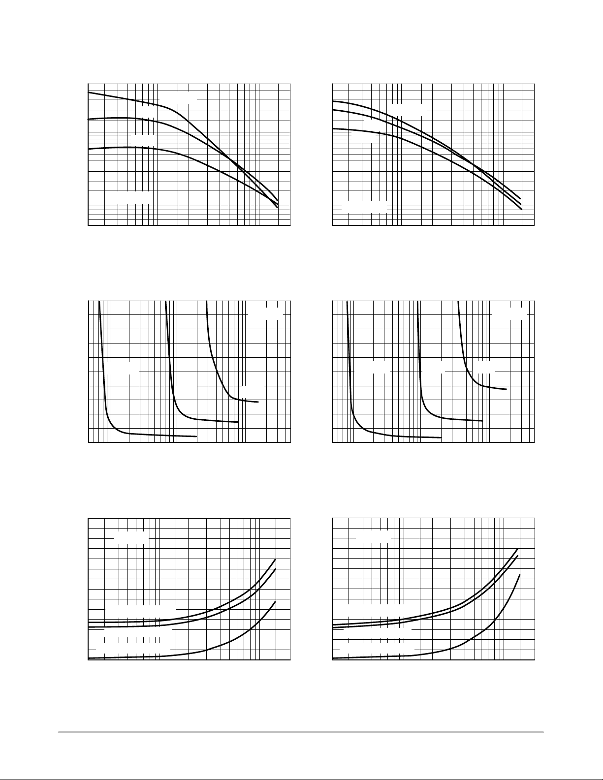
BD809 BD810
NPN
BD809
500
T
= 150°C
J
200
100
, DC CURRENT GAIN
FE
h
50
20
10
5.0
25°C
-55°C
VCE = 2.0 V
0.50.2 101.0 2.0
IC, COLLECTOR CURRENT (AMP)
5.0 0.50.2 101.0 2.0 205.0
Figure 3. DC Current Gain
2.0
1.8
1.6
1.4
1.2
IC = 1.0 A
4.0 A 8.0 A
0
5.0 100 5000
10
20 50
IB, BASE CURRENT (mA)
, COLLECTOR-EMITTER VOLTAGE (VOLTS)
CE
V
1.0
0.8
0.6
0.4
0.2
T
Figure 4. Collector Saturation Region
PNP
BD810
500
T
200
100
50
, DC CURRENT GAIN
20
FE
h
10
20
= 25°C
J
20001000200 500 5000
5.0
2.0
1.8
1.6
1.4
1.2
1.0
0.8
0.6
0.4
0.2
, COLLECTOR-EMITTER VOLTAGE (VOLTS)
CE
V
0
5.0 100
25°C
-55°C
VCE = 2.0 V
IC = 1.0 A
10
= 150°C
J
IC, COLLECTOR CURRENT (AMP)
4.0 A 8.0 A
20 50 20001000200 500
IB, BASE CURRENT (mA)
T
= 25°C
J
2.8
T
2.4
2.0
1.6
1.2
V, VOLTAGE (VOLTS)
0.8
0.4
0
0.2 0.5 2.0 20101.0 5.0
= 25°C
J
V
= IC/IB = 10
BE(sat)
VBE @ VCE = 2.0 V
V
@ IC/IB = 10
CE(sat)
IC, COLLECTOR CURRENT (AMP)
2.8
2.4
2.0
1.6
1.2
V, VOLTAGE (VOLTS)
V
0.8
0.4
V
0
0.2 0.5 2.0 20101.0 5.0
Figure 5. “On” Voltages
http://onsemi.com
3
T
= 25°C
J
@ IC/IB = 10
BE(sat)
VBE @ VCE = 2.0 V
@ IC/IB = 10
CE(sat)
IC, COLLECTOR CURRENT (AMP)
Page 4

1.0
0
0.7
0.5
0.3
0.2
0.1
0.07
0.05
THERMAL RESISTANCE
0.03
0.02
r(t), NORMALIZED EFFECTIVE TRANSIENT
0.01
0.01
D = 0.5
0.05
0.02
0.01
0.02 0.03
BD809 BD810
0.2
0.1
P
SINGLE
θJC(t) = r(t) θ
D CURVES APPLY FOR POWER
SINGLE PULSE
0.05 0.1 0.2 0.3 0.5 1.0 2.0 3.0 5.0 20 30 50 100 200 300 100
t, PULSE WIDTH (ms)
PULSE TRAIN SHOWN
READ TIME AT t
T
J(pk)
- TC = P
JC
1
(pk) θJC
PULSE
(t)
Figure 6. Thermal Response
(pk)
t
1
t
2
DUTY CYCLE, D = t1/t
2
500
Note 1:
There are two limitations on the power handling ability of
a transistor: average junction temperature and second
breakdown. Safe operating area curves indicate IC – V
CE
limits of the transistor that must be observed for reliable
operation, i.e., the transistor must not be subjected to greater
dissipation than the curves indicate.
The data of Figure 1 is based on T
= 150C; TC is
J(pk)
variable depending on conditions. Second breakdown pulse
limits are valid for duty cycles to 10% provided T
J(pk)
150C. At high case temperatures, thermal limitations
will reduce the power that can be handled to values less than
the limitations imposed by second breakdown.
http://onsemi.com
4
Page 5

Notes
BD809 BD810
http://onsemi.com
5
Page 6

Notes
BD809 BD810
http://onsemi.com
6
Page 7

BD809 BD810
PACKAGE DIMENSIONS
TO–220
CASE 221A–09
ISSUE AA
SEATING
–T–
PLANE
B
4
Q
123
F
T
A
U
C
S
H
K
Z
L
V
R
J
G
D
N
STYLE 1:
PIN 1. BASE
2. COLLECTOR
3. EMITTER
4. COLLECTOR
NOTES:
1. DIMENSIONING AND TOLERANCING PER ANSI
Y14.5M, 1982.
2. CONTROLLING DIMENSION: INCH.
3. DIMENSION Z DEFINES A ZONE WHERE ALL
BODY AND LEAD IRREGULARITIES ARE
ALLOWED.
DIM MIN MAX MIN MAX
A 0.570 0.620 14.48 15.75
B 0.380 0.405 9.66 10.28
C 0.160 0.190 4.07 4.82
D 0.025 0.035 0.64 0.88
F 0.142 0.147 3.61 3.73
G 0.095 0.105 2.42 2.66
H 0.110 0.155 2.80 3.93
J 0.018 0.025 0.46 0.64
K 0.500 0.562 12.70 14.27
L 0.045 0.060 1.15 1.52
N 0.190 0.210 4.83 5.33
Q 0.100 0.120 2.54 3.04
R 0.080 0.110 2.04 2.79
S 0.045 0.055 1.15 1.39
T 0.235 0.255 5.97 6.47
U 0.000 0.050 0.00 1.27
V 0.045 --- 1.15 ---
Z --- 0.080 --- 2.04
MILLIMETERSINCHES
http://onsemi.com
7
Page 8

BD809 BD810
ON Semiconductor and are registered trademarks of Semiconductor Components Industries, LLC (SCILLC). SCILLC reserves the right to make
changes without further notice to any products herein. SCILLC makes no warranty, representation or guarantee regarding the suitability of its products for any
particular purpose, nor does SCILLC assume any liability arising out of the application or use of any product or circuit, and specifically disclaims any and all
liability, including without limitation special, consequential or incidental damages. “Typical” parameters which may be provided in SCILLC data sheets and/or
specifications can and do vary in different applications and actual performance may vary over time. All operating parameters, including “Typicals” must be
validated for each customer application by customer’s technical experts. SCILLC does not convey any license under its patent rights nor the rights of others.
SCILLC products are not designed, intended, or authorized for use as components in systems intended for surgical implant into the body, or other applications
intended to support or sustain life, or for any other application in which the failure of the SCILLC product could create a situation where personal injury or death
may occur. Should Buyer purchase or use SCILLC products for any such unintended or unauthorized application, Buyer shall indemnify and hold SCILLC
and its officers, employees, subsidiaries, affiliates, and distributors harmless against all claims, costs, damages, and expenses, and reasonable attorney fees
arising out of, directly or indirectly, any claim of personal injury or death associated with such unintended or unauthorized use, even if such claim alleges that
SCILLC was negligent regarding the design or manufacture of the part. SCILLC is an Equal Opportunity/Affirmative Action Employer.
PUBLICATION ORDERING INFORMATION
Literature Fulfillment:
Literature Distribution Center for ON Semiconductor
P.O. Box 5163, Denver, Colorado 80217 USA
Phone: 303–675–2175 or 800–344–3860 Toll Free USA/Canada
Fax: 303–675–2176 or 800–344–3867 Toll Free USA/Canada
Email: ONlit@hibbertco.com
N. American Technical Support: 800–282–9855 Toll Free USA/Canada
http://onsemi.com
JAPAN: ON Semiconductor, Japan Customer Focus Center
4–32–1 Nishi–Gotanda, Shinagawa–ku, Tokyo, Japan 141–0031
Phone: 81–3–5740–2700
Email: r14525@onsemi.com
ON Semiconductor Website: http://onsemi.com
For additional information, please contact your local
Sales Representative.
BD809/D
8
 Loading...