

Page 1
1
Motorola Bipolar Power Transistor Device Data
. . . designed for low power audio amplifier and low–current, high speed switching
applications.
• High Collector–Emitter Sustaining Voltage —
V
CEO(sus)
= 100 Vdc (Min)
• High DC Current Gain @ IC = 200 mAdc
hFE = 40–250
• Low Collector–Emitter Saturation Voltage —
V
CE(sat)
= 0.5 Vdc (Max) @ IC = 500 mAdc
• High Current Gain — Bandwidth Product —
fT = 40 MHz (Min) @ IC = 100 mAdc)
*MAXIMUM RATINGS
Rating
Symbol
Max
Unit
Collector–Emitter V oltage
V
CEO
100
Vdc
Collector–Base Voltage
V
CB
100
Vdc
Emitter–Base Voltage
V
EBO
6.0
Vdc
ОООООООООО
Î
Collector Current — Continuous
— Peak
ÎÎÎ
Î
I
C
ÎÎÎÎ
Î
4.0
8.0
Î
Î
Adc
Base Current
I
B
1.0
Adc
ОООООООООО
Î
Total Power Dissipation @ TC = 25_C
Derate above 25_C
ÎÎÎ
Î
P
D
ÎÎÎÎ
Î
15
0.12
Î
Î
Watts
W/_C
Operating and Storage Junction
T emperature Range
TJ,T
stg
–65 to +150
_
C
ООООООООООООООООООООО
Î
THERMAL CHARACTERISTICS
Characteristic
Symbol
Max
Unit
Thermal Resistance, Junction to Case
R
θJC
8.34
_
C/W
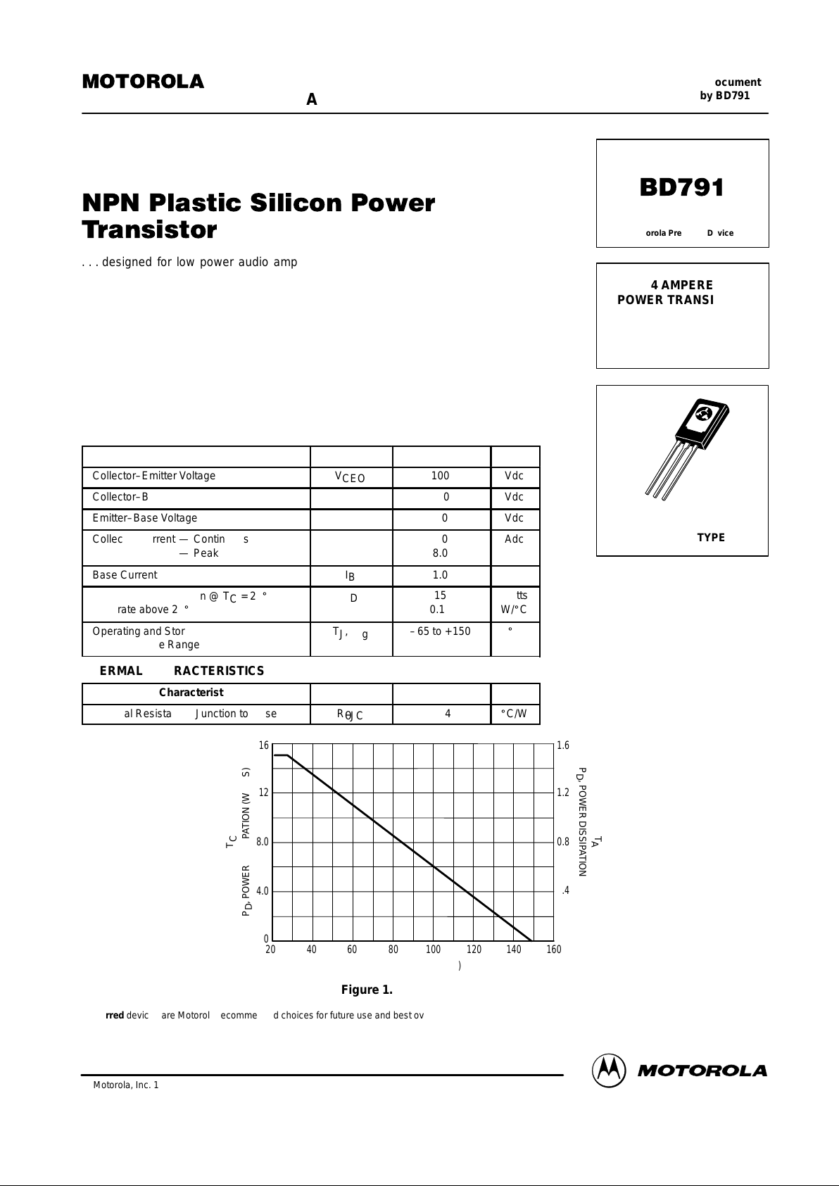
16
12
0
20 40 60 100 120 140 160
Figure 1. Power Derating
T, TEMPERATURE (°C)
80
4.0
8.0
1.6
1.2
0
0.4
0.8
T
A
T
C
P
D
, POWER DISSIPATION (WATTS)
P
D
, POWER DISSIPATION (WATTS)
Preferred devices are Motorola recommended choices for future use and best overall value.
SEMICONDUCTOR TECHNICAL DATA
Order this document
by BD791/D
Motorola, Inc. 1998
Motorola Preferred Device
4 AMPERE
POWER TRANSISTOR
SILICON
100 VOLTS
15 WATTS
CASE 77–09
TO–225AA TYPE
Page 2
BD791
2
Motorola Bipolar Power Transistor Device Data
*ELECTRICAL CHARACTERISTICS (T
C
= 25_C unless otherwise noted)
Characteristic
ÎÎÎÎ
Symbol
Min
Max
ÎÎÎ
Unit
OFF CHARACTERISTICS
ООООООООООООООООООООО
Î
Collector–Emitter Sustaining Voltage (1)
(IC = 10 mAdc, IB = 0)
ÎÎÎÎ
ÎÎÎ
Î
V
CEO(sus)
ÎÎ
Î
100
ÎÎ
Î
—
ÎÎÎ
ÎÎ
Î
Vdc
ООООООООООООООООООООО
Î
Collector Cutoff Current
(VCE = 50 Vdc, IB = 0)
ÎÎÎ
Î
I
CEO
ÎÎ
Î
—
ÎÎ
Î
100
ÎÎ
Î
µAdc
ООООООООООООООООООООО
Î
Collector Cutoff Current
(VCE = 100 Vdc, V
BE(off)
= 1.5 Vdc)
(VCE = 50 Vdc, V
BE(off)
= 1.5 Vdc, TC = 125_C)
ÎÎÎ
Î
I
CEX
ÎÎ
Î
—
—
ÎÎ
Î
1.0
0.1
ÎÎ
Î
µAdc
mAdc
Emitter Cutoff Current (VEB = 6.0 Vdc, IC = 0)
I
EBO
—
1.0
µAdc
ON CHARACTERISTICS (1)
ООООООООООООООООООООО
Î
ООООООООООООООООООООО
Î
ООООООООООООООООООООО
Î
DC Current Gain
(IC = 200 mAdc, VCE = 3 0 Vdc)
(IC = 1.0 Adc, VCE = 3.0 Vdc)
(IC = 2.0 Adc, VCE = 3.0 Vdc)
(IC = 4.0 Adc, VCE = 3.0 Vdc)
ÎÎÎ
Î
ÎÎÎ
Î
ÎÎÎ
Î
h
FE
ÎÎ
Î
ÎÎ
Î
ÎÎ
Î
40
20
10
5.0
ÎÎ
Î
ÎÎ
Î
ÎÎ
Î
250
—
—
—
ÎÎ
Î
ÎÎ
Î
ÎÎ
Î
—
ООООООООООООООООООООО
Î
ООООООООООООООООООООО
Î
ООООООООООООООООООООО
Î
Collector Emitter Saturation Voltage
(IC = 500 mAdc, IB = 50 mAdc)
(IC = 1.0 Adc, IB = 100 mAdc)
(IC = 2.0 Adc, IB = 200 mAdc)
(IC = 4.0 Adc, IB = 800 mAdc)
ÎÎÎ
Î
ÎÎÎ
Î
ÎÎÎ
Î
V
CE(sat)
ÎÎ
Î
ÎÎ
Î
ÎÎ
Î
—
—
—
—
ÎÎ
Î
ÎÎ
Î
ÎÎ
Î
0.5
1.0
2.5
3.0
ÎÎ
Î
ÎÎ
Î
ÎÎ
Î
Vdc
Base–Emitter Saturation Voltage (IC = 2.0 Adc, IB = 200 mAdc)
V
BE(sat)
—
1.8
Vdc
Base–Emitter On Voltage (IC = 200 mAdc, VCE = 3.0 Vdc)
V
BE(on)
—
1.5
Vdc
DYNAMIC CHARACTERISTICS
Current–Gain — Bandwidth Product
(IC = 100 mAdc, VCE = 10 Vdc, f = 10 MHz)
f
T
40
—
MHz
ООООООООООООООООООООО
Î
Output Capacitance
(VCB = 10 Vdc, IC = 0, f = 0.1 MHz)
ÎÎÎ
Î
C
ob
ÎÎ
Î
—
ÎÎ
Î
50
ÎÎ
Î
pF
ООООООООООООООООООООО
Î
Small–Signal Current Gain
(IC = 200 mAdc, VCE = 10 Vdc, f = 1.0 kHz)
ÎÎÎ
Î
h
fe
ÎÎ
Î
10
ÎÎ
Î
—
ÎÎ
Î
—
*Indicates JEDEC Registered Data.
(1) Pulse Test: Pulse Width v 300 µs, Duty Cycle v 2.0%.
Figure 2. Switching Time Test Circuit
500
0.04
Figure 3. Turn–On Time
IC, COLLECTOR CURRENT (AMP)
t, TIME (ns)
70
30
20
5.0
0.06 0.2 0.4 0.6
td @ V
BE(off)
= 5.0 V
TJ = 25°C
VCC = 30 V
IC/IB = 10
+ 11 V
0
+ 30 V
SCOPE
R
B
– 4 V
tr, tf
v
10 ns
DUTY CYCLE = 1.0%
R
C
t
r
7.0
10
1.0 4.0
D1 MUST BE FAST RECOVERY TYPE, eg
MBR340 USED ABOVE IB
[
100 mA
MSD6100 USED BELOW IB
[
100 mA
FOR PNP TEST CIRCUIT, REVERSE ALL POLARITIES.
25 µs
– 9.0 V
D
1
51
RB AND RC VARIED TO OBT AIN DESIRED CURRENT LEVELS
V
CC
300
200
100
50
0.1 2.0
Page 3

BD791
3
Motorola Bipolar Power Transistor Device Data
Figure 4. Thermal Response
t, TIME (ms)
1.0
0.01
0.7
0.5
0.3
0.2
0.1
0.07
0.05
0.03
0.02
0.02 0.05 0.1 0.2 0.5 1.0 2.0 5.0 10 20 50 100 200
R
θ
JC(t)
= r(t) R
θ
JC
R
θ
JC
= 8.34°C/W MAX
D CURVES APPLY FOR POWER
PULSE TRAIN SHOWN
READ TIME AT t
1
T
J(pk)
– TC = P
(pk)
R
θ
JC(t)
P
(pk)
t
1
t
2
DUTY CYCLE, D = t1/t
2
D = 0.5
0 (SINGLE PULSE)
0.2
0.05
0.1
0.02
0.01
r(t), TRANSIENT THERMAL RESIST ANCE
(NORMALIZED)
I
C
, COLLECTOR CURRENT (AMP)
Figure 5. Active Region Safe Operating Area
10
1.0
VCE, COLLECTOR–EMITTER VOL TAGE (VOLTS)
5.0
2.0
0.5
0.01
2.0 5.0 10 50 100
BONDING WIRE LIMITED
THERMALL Y LIMITED @ TC = 25
°
C
(SINGLE PULSE)
SECOND BREAKDOWN LIMITED
0.05
0.02
20
CURVES APPLY BELOW RATED V
CEO
TJ = 150°C
dc
5.0 ms
1.0 ms
500 µs
100 µs
1.0
0.1
30 703.0 7.0
There are two limitations on the power handling ability of a
transistor: average junction temperature and second breakdown. Safe operating area curves indicate IC – VCE limits of
the transistor that must be observed for reliable operation,
i.e., the transistor must not be subjected to greater dissipation than the curves indicate.
The data of Figure 5 is based on T
J(pk)
= 150_C: TC is
variable depending on conditions. Second breakdown pulse
limits are valid for duty cycles to 10% provided T
J(pk)
v
150_C, T
J(pk)
may be calculated from the data in Figure 4. At high case temperatures, thermal limitations will reduce the power that can be handled to values less than the
limitations imposed by second breakdown.
0.04
Figure 6. Turn–Off Time
IC, COLLECTOR CURRENT (AMP)
t, TIME (ns)
0.06 0.1 0.2 0.6 1.0 2.0 4.0
TJ = 25°C
VCC = 30 V
IC/IB = 10
IB1 = I
B2
t
s
0.4
t
f
2000
20
700
100
200
1000
500
300
30
50
70
200
1.0
Figure 7. Capacitance
VR, REVERSE VOLTAGE (VOLTS)
10
2.0 3.0 5.0 7.0 20 30 10010
C, CAPACITANCE (pF)
100
70
50
30
TJ = 25°C
C
ib
C
ob
20
50 70
Page 4

BD791
4
Motorola Bipolar Power Transistor Device Data
500
0.04
Figure 8. DC Current Gain
IC, COLLECTOR CURRENT (AMP)
0.1 0.2 0.4 0.6 1.0 2.0
100
50
30
300
70
h
FE
, DC CURRENT GAIN
TJ = 150°C
25°C
–55°C
200
20
4.0
VCE = 1.0 V
VCE = 3.0 V
0.06
5.0
7.0
1.4
0.04
IC, COLLECTOR CURRENT (AMP)
0.2 0.6 2.0 4.0
0.6
0.4
0
TJ = 25°C
V
BE(sat)
@ IC/IB = 10
V
CE(sat)
V, VOLTAGE (VOLTS)
Figure 9. “On” Voltage
0.1 1.00.4
1.0
0.8
V
BE(on)
@ VCE = 3.0 V
0.06
1.2
0.2
IC/IB = 10
5.0
+2.5
Figure 10. Temperature Coefficient
IC, COLLECTOR CURRENT (AMP)
V
, TEMPERATURE COEFFICIENTS (mV/ C)
°θ
+2.0
+1.5
+0.5
0
–0.5
–1.0
–1.5
–2.0
–2.5
θVB FOR V
BE
*
θ
VC
FOR V
CE(sat)
*APPLIES FOR IC/IB
≤
h
FE/3
+1.0
25
°
C to 150°C
– 55°C to 25°C
25°C to 150°C
– 55°C to 25°C
0.04 0.2 0.6 2.0 4.00.1 1.00.40.06
Page 5

BD791
5
Motorola Bipolar Power Transistor Device Data
P ACKAGE DIMENSIONS
CASE 77–09
TO–225AA TYPE
ISSUE W
STYLE 1:
PIN 1. EMITTER
2. COLLECTOR
3. BASE
NOTES:
1. DIMENSIONING AND TOLERANCING PER ANSI
Y14.5M, 1982.
2. CONTROLLING DIMENSION: INCH.
–B–
–A–
M
K
F
C
Q
H
V
G
S
D
J
R
U
132
2 PL
M
A
M
0.25 (0.010) B
M
M
A
M
0.25 (0.010) B
M
DIM MIN MAX MIN MAX
MILLIMETERSINCHES
A 0.425 0.435 10.80 11.04
B 0.295 0.305 7.50 7.74
C 0.095 0.105 2.42 2.66
D 0.020 0.026 0.51 0.66
F 0.115 0.130 2.93 3.30
G 0.094 BSC 2.39 BSC
H 0.050 0.095 1.27 2.41
J 0.015 0.025 0.39 0.63
K 0.575 0.655 14.61 16.63
M 5 TYP 5 TYP
Q 0.148 0.158 3.76 4.01
R 0.045 0.065 1.15 1.65
S 0.025 0.035 0.64 0.88
U 0.145 0.155 3.69 3.93
V 0.040 ––– 1.02 –––
__
Page 6

BD791
6
Motorola Bipolar Power Transistor Device Data
Motorola reserves the right to make changes without further notice to any products herein. Motorola makes no warranty , representation or guarantee regarding
the suitability of its products for any particular purpose, nor does Motorola assume any liability arising out of the application or use of any product or circuit, and
specifically disclaims any and all liability, including without limitation consequential or incidental damages. “T ypical” parameters which may be provided in Motorola
data sheets and/or specifications can and do vary in different applications and actual performance may vary over time. All operating parameters, including “Typicals”
must be validated for each customer application by customer’s technical experts. Motorola does not convey any license under its patent rights nor the rights of
others. Motorola products are not designed, intended, or authorized for use as components in systems intended for surgical implant into the body, or other
applications intended to support or sustain life, or for any other application in which the failure of the Motorola product could create a situation where personal injury
or death may occur. Should Buyer purchase or use Motorola products for any such unintended or unauthorized application, Buyer shall indemnify and hold Motorola
and its officers, employees, subsidiaries, affiliates, and distributors harmless against all claims, costs, damages, and expenses, and reasonable attorney fees
arising out of, directly or indirectly, any claim of personal injury or death associated with such unintended or unauthorized use, even if such claim alleges that
Motorola was negligent regarding the design or manufacture of the part. Motorola and are registered trademarks of Motorola, Inc. Motorola, Inc. is an Equal
Opportunity/Affirmative Action Employer.
Mfax is a trademark of Motorola, Inc.
How to reach us:
USA/EUROPE/Locations Not Listed: Motorola Literature Distribution; JAPAN: Nippon Motorola Ltd.; SPD, Strategic Planning Office, 141,
P.O. Box 5405, Denver, Colorado 80217. 1–303–675–2140 or 1–800–441–2447 4–32–1 Nishi–Gotanda, Shinagawa–ku, Tokyo, Japan. 81–3–5487–8488
Customer Focus Center: 1–800–521–6274
Mfax: RMFAX0@email.sps.mot.com – TOUCHTONE 1–602–244–6609 ASIA/PACIFIC: Motorola Semiconductors H.K. Ltd.; 8B Tai Ping Industrial Park,
Moto rola Fax Back System – US & Canada ONLY 1–800–774–1848 51 Ting Kok Road, T ai Po, N.T., Hong Kong. 852–26629298
– http://sps.motorola.com/mfax/
HOME PAGE: http://motorola.com/sps/
BD791/D
◊
 Loading...