

Page 1
1/4
STRUCTURE Silicon Monolithic Integrated Circuit
PRODUCT SERIES 1ch. Reversible Motor Driver
TYPE BD6736FV
FEATURES ・Full-ON type 1ch. H-bridge Driver
zAbsolute maximum ratings (Ta=25°C)
Parameter Symbol Limit Unit
Power supply voltage VCC -0.5 to +10.0 V
Motor power supply voltage VM -0.5 to +10.0 V
Charge pump step-up
power supply voltage
Control input voltage VIN -0.5 to VCC+0.5 V
Power dissipation Pd 930※1 mW
Operating temperature range Topr -30 to +75 °C
Junction temperature Tjmax 150 °C
Storage temperature range Tstg -55 to +150 °C
H-bridge output current DC Iout -1000 to +1000※2 mA
H-bridge output current (100msec) Iopeak -3200 to +3200※2 mA
※1
Reduced by 7.44mW/°C over 25°C, when mounted on a glass epoxy board (70mm × 70mm × 1.6mm)
※2
Must not exceed Pd, ASO, or Tjmax of 150°C.
VBST -0.5 to +15.0 V
zOperating Conditions (Ta= -30°C to +75°C)
Parameter Symbol Min. Typ. Max. Unit
Power supply voltage VCC 2.0 5.0 9.0 V
Motor power supply voltage VM 2.0 5.0 9.0 V
Control input voltage VIN 0 - VCC V
Logic input frequency FIN 0 - 100 kHz
Min. logic pulse width TIN 0.5 - - μs
The product described in this specification is a strategic product (and/or service) subject to COCOM regulations.
It should not be exported without authorization from the appropriate government authorities.
This product isn’t designed for protection against radioactive rays.
Status of this document: The Japanese version of this document is the formal specification. A customer may use this translation
version only for a reference to help reading the formal version. If there are any differences in translation version of this document,
formal version takes priority.
REV. C
Page 2
2/4
zBD6736FV Electrical Characteristics (Unless otherwise specified Ta=25°C, VCC=5.0V, VM=5.0V)
Parameter Symbol
Overall
Circuit current
during standby operation
Circuit current ICC 0.5 2.0 4.0 mA PS=H, FIN=100kHz
Power saving
High-level input voltage VPSH 2.0 - VCC V
Low-level input voltage VPSL -0.3 - 0.5 V
High-level input current IPSH 25 50 100 μA VPSH=5V
Low-level input current IPSL -1 0 1 μA VPSL=0V
Control input
High-level input voltage VINH 2.0 - VCC V
Low-level input voltage VINL -0.3 - 0.7 V
High-level input current IINH 25 50 100 μA VINH=5V
Low-level input current IINL -1 0 1 μA VINL=0V
UVLO
UVLO voltage VUVLO 1.5 - 1.9 V
Full-ON Drive block
Output ON-Resistance RON - 0.35 0.5 Ω Io=±500mA on high and low sides in total
ICCST - 0 1 μA PS=0V
Min. Typ. Max.
Limit
Unit Conditions
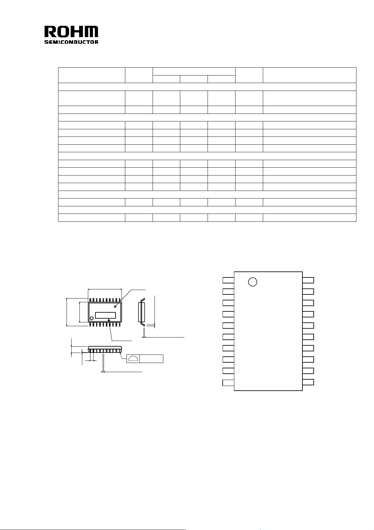
zPackage Outline zPin Arrangement (Top View)
1
6.4 ± 0.3
6.5 ± 0.2
20
4.4 ± 0.2
1
BD6736
11
10
Lot No.
Type name
0.3Min.
0.15 ± 0.1
1.15 ± 0.1
0.1
0.65
0.22 ± 0.1
0.1
VM
2
N.C.
3
OUTA
4
OUTA
MGND
5
MGND
6
OUTB
7
OUTB
8
VM
9
10
GND
Fig.1 SSOP-B20 Package (Unit: mm)
Fig.2 BD6736FV Pin Arrangement (Top View)
VCC
PS
INA
INB
PWM
CPL1
CPL2
CPH1
CPH2
BST
20
19
18
17
16
15
14
13
12
11
REV. C
Page 3

3/4
zBlock Diagram zPin No. and Pin Name
PS
19
Power Save
INA
INB
18
17
16
PWM
Logic
Power Save
1~100uF
Level Shift
&
Pre Driver
BST
VCC
20
BandGapTSD & UVLO
9
4
8
6
1~100uF
VM
OUTA
OUTB
MGND
H bridge
1
3
F
7
5
OSC Charge Pump Charge Pump
10
GND
14
15 13 11
CPL1 CPL2
CPH1
12
CPH2
BST
Fig.3 BD6736FV Block Diagram
No. Pin ame
1
2
3
4
5
6
7
8
9
10
11
12
13
14
15
16
17
18
19
20
VM
N.C.
OUTA
OUTA
MGND
MGND
OUTB
OUTB
VM
GND
BST
CPH2
CPH1
CPL2
CPL1
PWM
INB
INA
PS
VCC
I/O Truth Table
z
BD6736FV I/O Truth Table
INPUT OUTPUT
Input mode
EN/IN
IN/IN L
- L X X X Z Z
L: Low, H: High, X: Don’t care, Z: High Impedance
PS
H
PWM
EN
H
INA INB OUTA OUTB
L X L L
H L H L
H H L H
L L Z Z
H L H L
L H L H
H H L L
REV. C
Page 4

4/4
zOperation Notes
(1) Absolute maximum ratings
Use of the IC in excess of absolute maximum ratings such as the applied voltage or operating temperature range (Topr) may
result in IC damage. Assumptions should not be made regarding the state of the IC (short mode or open mode) when such
damage is suffered. The implementation of a physical safety measure such as a fuse should be considered when use of the IC in
a special mode where the absolute maximum ratings may be exceeded is anticipated.
(2) Power supply pins and lines
None of the VM line for the H-bridge is internally connected to the VCC power supply line, which is only for the control logic or
analog circuit. Therefore, the VM and VCC lines can be driven at different voltages. Although these lines can be connected to a
common power supply, do not open the power supply pin but connect it to the power supply externally.
Regenerated current may flow as a result of the motor's back electromotive force. Insert capacitors between the power supply
and ground pins to serve as a route for regenerated current. Determine the capacitance in full consideration of all the
characteristics of the electrolytic capacitor, because the electrolytic capacitor may loose some capacitance at low temperatures.
If the connected power supply does not have sufficient current absorption capacity, regenerative current will cause the voltage
on the power supply line to rise, which combined with the product and its peripheral circuitry may exceed the absolute maximum
ratings. It is recommended to implement a physical safety measure such as the insertion of a voltage clamp diode between the
power supply and ground pins.
For this IC with 2 power supplies and a part consists of the CMOS block, it is possible that rush current may flow instantaneously
due to the internal powering sequence and delays, and to the unstable internal logic, respectively. Therefore, give special
consideration to power coupling capacitance, width of power and ground wirings, and routing of wiring.
(3) Ground pins and lines
Ensure a minimum GND pin potential in all operating conditions. Make sure that no pins are at a voltage below the GND at any
time, regardless of whether it is a transient signal or not.
When using both small signal GND and large current MGND patterns, it is recommended to isolate the two ground patterns,
placing a single ground point at the application's reference point so that the pattern wiring resistance and voltage variations
caused by large currents do not cause variations in the small signal ground voltage. Be careful not to change the GND wiring
pattern of any external components, either.
The power supply and ground lines must be as short and thick as possible to reduce line impedance.
(4) Thermal design
Use a thermal design that allows for a sufficient margin in light of the power dissipation (Pd) in actual operating conditions.
(5) Actions in strong magnetic field
Use caution when using the IC in the presence of a strong magnetic field as doing so may cause the IC to malfunction.
(6) ASO
When using the IC, set the output transistor for the motor so that it does not exceed absolute maximum ratings or ASO.
(7) Thermal shutdown circuit
This IC incorporates a TSD (thermal shutdown) circuit. If the temperature of the chip reaches the following temperature,
the motor coil output will be opened. The TSD circuit is designed only to shut the IC off to prevent runaway thermal operation.
It is not designed to protect the IC or guarantee its operation. Do not continue to use the IC after operating this circuit or use
the IC in an environment where the operation of this circuit is assumed.
TSD ON temperature [°C] (Typ.) Hysteresis temperature [°C] (Typ.)
(8) Application example
The application circuit is recommended for use. Make sure to confirm the adequacy of the characteristics. When using the circuit
with changes to the external circuit constants, make sure to leave an adequate margin for external components including static
and transitional characteristics as well as dispersion of the IC.
160 20
REV. C
Page 5

Appendix
No copying or reproduction of this document, in part or in whole, is permitted without the consent of ROHM
CO.,LTD.
The content specified herein is subject to change for improvement without notice.
The content specified herein is for the purpose of introducing ROHM's products (hereinafter "Products"). If you
wish to use any such Product, please be sure to refer to the specifications, which can be obtained from ROHM
upon request.
Examples of application circuits, circuit constants and any other information contained herein illustrate the
standard usage and operations of the Products. The peripheral conditions must be taken into account
when designing circuits for mass production.
Great care was taken in ensuring the accuracy of the information specified in this document. However, should
you incur any damage arising from any inaccuracy or misprint of such information, ROHM shall bear no re-
sponsibility for such damage.
The technical information specified herein is intended only to show the typical functions of and examples
of application circuits for the Products. ROHM does not grant you, explicitly or implicitly, any license to
use or exercise intellectual property or other rights held by ROHM and other parties. ROHM shall bear no re-
sponsibility whatsoever for any dispute arising from the use of such technical information.
The Products specified in this document are intended to be used with general-use electronic equipment
or devices (such as audio visual equipment, office-automation equipment, communication devices, elec-
tronic appliances and amusement devices).
The Products are not designed to be radiation tolerant.
While ROHM always makes efforts to enhance the quality and reliability of its Products, a Product may fail or
malfunction for a variety of reasons.
Please be sure to implement in your equipment using the Products safety measures to guard against the
possibility of physical injury, fire or any other damage caused in the event of the failure of any Product, such as
derating, redundancy, fire control and fail-safe designs. ROHM shall bear no responsibility whatsoever for your
use of any Product outside of the prescribed scope or not in accordance with the instruction manual.
The Products are not designed or manufactured to be used with any equipment, device or system
which requires an extremely high level of reliability the failure or malfunction of which may result in a direct
threat to human life or create a risk of human injury (such as a medical instrument, transportation equipment,
aerospace machinery, nuclear-reactor controller, fuel-controller or other safety device). ROHM shall bear
no responsibility in any way for use of any of the Products for the above special purposes. If a Product is intend-
ed to be used for any such special purpose, please contact a ROHM sales representative before purchasing.
If you intend to export or ship overseas any Product or technology specified herein that may be controlled under
the Foreign Exchange and the Foreign Trade Law, you will be required to obtain a license or permit under the Law.
Notes
Thank you for your accessing to ROHM product informations.
More detail product informations and catalogs are available, please contact your nearest sales office.
ROHM Customer Support System
www.rohm.com
Copyright © 2009 ROHM CO.,LTD.
21 Saiin Mizosaki-cho, Ukyo-ku, Kyoto 615-8585, Japan
THE AMERICAS / EUROPE / ASIA / JAPAN
Contact us : webmaster@ rohm.co. jp
TEL : +81-75-311-2121
FAX : +81-75-315-0172
Appendix-Rev4.0
 Loading...