

Page 1
BD439/BD440
BD441/BD442
COMPLEMENTARY SILICON POWER TRANSISTORS
■ SGS-THOMS O N PREF ERRE D SA LES TYP E S
■ COMPLEM EN TARY PNP - NPN DEVICES
DESCRIPTION
The BD439 and BD441 are silicon epitaxial-base
NPN power transistors in Jedec SOT-32 plastic
package, intented for use in power linear and
switching applications.
The complementary PNP types are BD440, and
BD442 respectively.
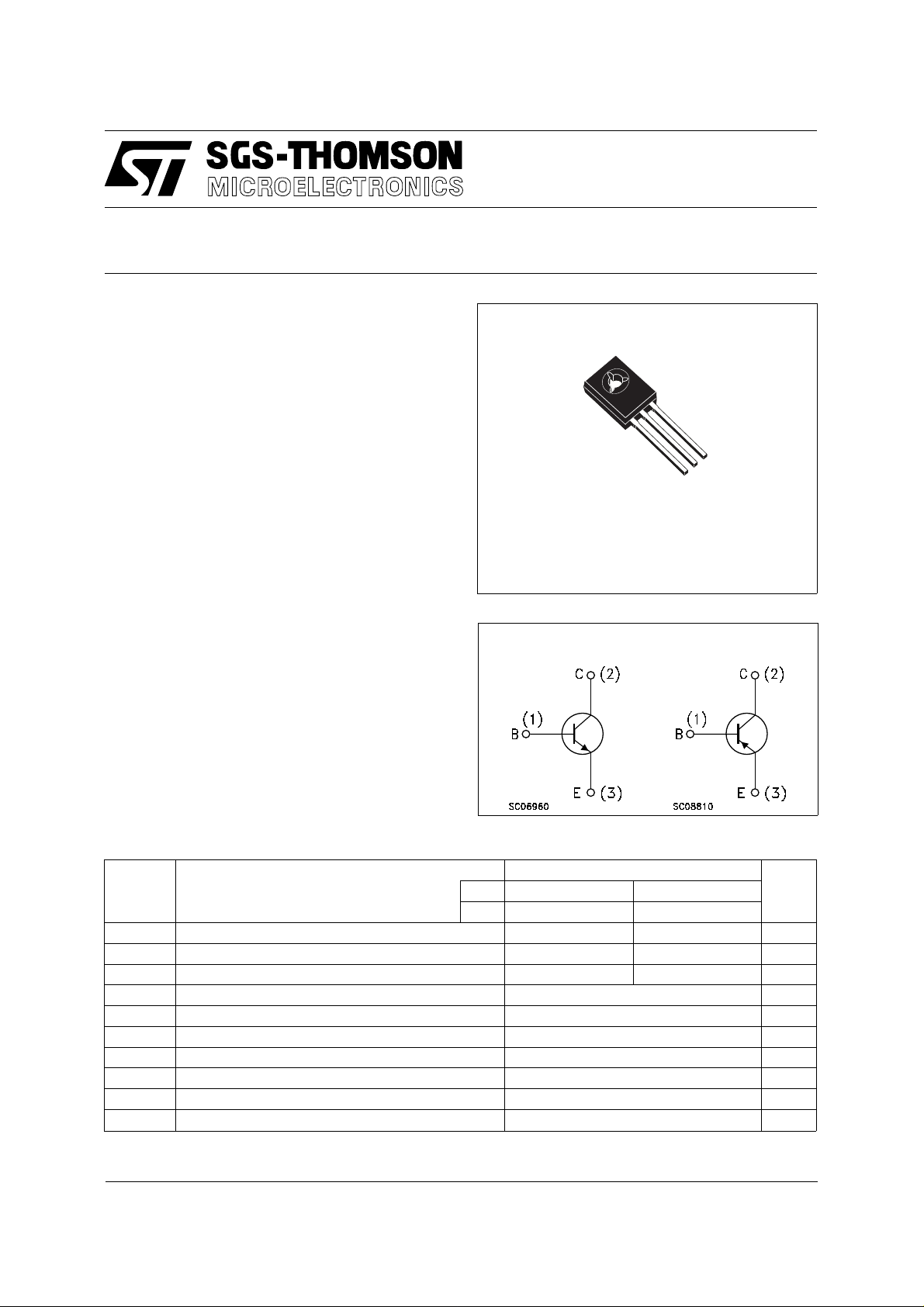
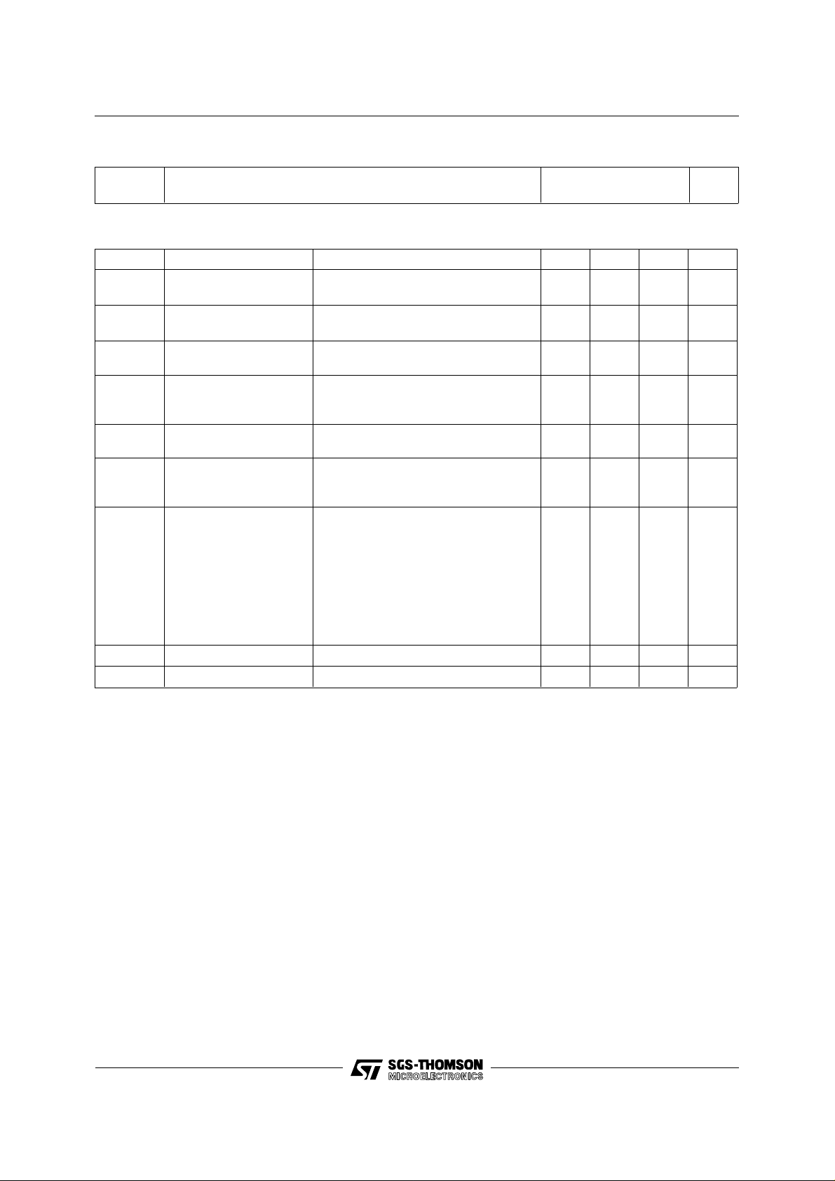
SOT-32
1
2
3
INTERNAL SCHEMATIC DIAGRAM
ABSOLUTE MAXIMUM RATING S
Symbol Parameter Value Unit
NPN BD439 BD441
PNP BD440 BD442
V
V
V
V
I
P
T
For PNP types voltage and current values are negative.
Collector-Base Voltage (IE = 0) 60 80 V
CBO
Collector-Emitter Voltage (VBE = 0) 60 80 V
CES
Collector-Emitter Voltage (IB = 0) 60 80 V
CEO
Emitter-Base Voltage (IC = 0) 5 V
EBO
Collector Current 4 A
I
C
Collector Peak Current (t ≤ 10 ms) 7 A
CM
Base Current 1 A
I
B
Total Dissipation at Tc ≤ 25 oC36W
tot
Storage Temperature -65 to 150
stg
Max. Operating Junction Temperature 150
T
j
o
C
o
C
May 1997
1/4
Page 2
BD439/BD440/ BD441/BD 442
THERMAL DATA
R
thj-case
R
thj-amb
Thermal Resistance Junction-case Max
Thermal Resistance Junction-ambient Max
3.5
100
o
C/W
o
C/W
ELECTRICAL CHARACTERISTICS (T
= 25 oC unless otherwise specified)
case
Symbol Parameter Test Conditions Min. Typ. Max. Unit
I
CBO
I
CES
I
EBO
V
CEO(sus)
V
CE(sat)
V
BE
Collector Cut-off
Current (I
= 0)
E
Collector Cut-off
Current (V
BE
= 0)
Emitter Cut-off Current
(I
= 0)
C
∗ Collector-Emitter
Sustaining Voltage
(I
= 0)
B
∗ Collector-Emitter
Saturation Voltage
for BD439/440 V
for BD441/442 V
for BD439/440 V
for BD441/442 V
= 5 V 1 mA
V
EB
I
= 100 mA for DB439/440
C
for BD441/442
IC = 2 A IB = 0.2 A
= 60 V
CB
= 80 V
CB
= 60 V
CB
= 80 V
CB
∗ Base-Emitter Voltage IC = 10 mA VCE = 5 V
I
= 2 A VCE = 1 V
C
100
100
100
100
60
80
0.8 V
0.58
1.5
h
∗ DC Current Gain IC = 10 mA VCE = 5 V
FE
for BD439/440
for BD441/442
I
for BD439/440
for BD441/442
I
for BD439/440
for BD441/442
h
FE1/hFE2
∗ Pulsed: Pulse duration = 300 µs, duty cycle 1.5 %
∗ Matched Pair IC = 500 mA VCE = 1 V 1.4
f
Transition frequency IC = 250 mA VCE = 1 V 3 MHz
T
= 500 mA VCE = 1 V
C
= 2 A VCE = 1 V
C
20
15
40
40
25
15
130
130
140
140
µA
µA
µA
µA
V
V
V
V
2/4
Page 3

0016114
BD439/BD44 0/BD441/BD442
SOT-32 (TO-126) MECHANICAL DATA
DIM.
MIN. TYP. MAX. MIN. TYP. MAX.
A 7.4 7.8 0.291 0.307
B 10.5 10.8 0.413 0.445
b 0.7 0.9 0.028 0.035
b1 0.49 0.75 0.019 0.030
C 2.4 2.7 0.040 0.106
c1 1.0 1.3 0.039 0.050
D 15.4 16.0 0.606 0.629
e2.2 0.087
e3 4.15 4.65 0.163 0.183
F3.8 0.150
G 3 3.2 0.118 0.126
H2.540.100
H2 2.15 0.084
mm inch
H2
3/4
Page 4

BD439/BD440/ BD441/BD442
Information furnished is believed to be accurate and reliable. However, SGS-THOMSON Microelectronics assumes no responsability for the
consequences of use of such information nor for any infringement of patents or other rights of third parties which may results from its use. No
license is granted by implication or ot h erwise under any patent or patent rights of SGS-THOMSON Microelectronics. Specifi cations mentioned
in this publication are subject to change without notice. This publication sup ersedes and replaces all information previously supplied.
SGS-THOMSON Microelectronics products are not authorized for use as critical components in life support devices or systems without express
written approval of SGS-THOMSON Microelectonics.
© 1997 SGS-THOMSON Microelectronics - Printed in Italy - All Rights Reserved
Australia - Brazil - Canada - China - France - Germany - Hong Kong - Italy - Japan - Korea - Malaysia - Malta - Morocco - The Netherlands -
Singapore - Spain - Sweden - Switzerland - Taiwan - Thailand - United Kingdom - U.S.A
SGS-THOMSON Microelectronics GROUP OF COMPANIES
. . .
4/4
 Loading...