

Page 1
NPN SILICON POWER TRANSISTOR
■ STMicroelectronicsPREFERRED
SALESTYPE
DESCRIPTION
The BD239C is a silicon epitaxial-base NPN
transistorin JedecTO-220 plasticpackage.
It is inteded for use in medium power linear and
switchingapplications.
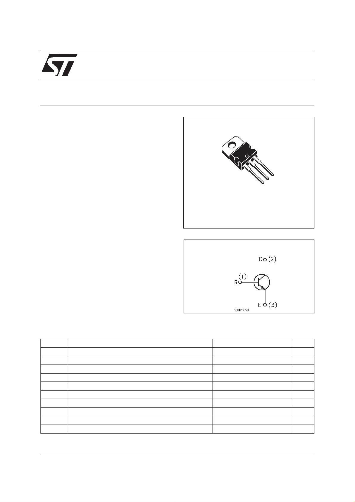
TO-220
BD239C
3
2
1
INTERNAL SCHEMATIC DIAGRAM
ABSOLUTE MAXIMUM RATINGS
Symbol Parameter Value Unit
V
V
V
I
P
P
T
Collect or-Emitter Voltage (RBE=100Ω)
CER
Collect or-Emitter Voltage (IB=0) 100 V
CEO
Emitter-Base Voltage (IC=0) 5 V
EBO
I
Collect or Curre nt 2 A
C
Collect or Peak Current 4 A
CM
I
Base Current 0.6 A
B
tot Tot al Dis sipation at T
tot Tot al Dis sipation at T
Storage Temperature -65 to150
stg
T
Max. O pe r ating Junctio n Tempe rature 150
j
≤ 25oC
c
≤ 25oC
amb
115 V
30 W
2W
o
C
o
C
April 1999
1/4
Page 2
BD239C
THERMAL DATA
R
thj-case
R
thj-amb
Ther mal Res ist an c e Junc tion-cas e Max
Ther mal Res ist an c e Junc tion-am bie nt Max
4.17
62.5
o
C/W
o
C/W
ELECTRICAL CHARACTERISTICS (T
=25oC unlessotherwise specified)
case
Symbol Parameter Test Conditions Min. Typ. Max. Unit
I
CES
I
CEO
I
EBO
V
CEO(sus)
Collec t or Cut -off
Current (V
BE
=0)
Collec t or Cut -off
Current (I
B
=0)
Emitt er Cut-off Current
(I
=0)
C
∗ Co llector- E m itter
V
=100V 0.2 mA
CE
V
=60V 0.3 mA
CE
=5V 1 mA
V
EB
IC= 30 mA 100 V
Sust aining Voltage
∗ Collec t or -Emit t er
V
CE(sat)
IC=1A IB= 0.2 A 0.7 V
Saturation Voltage
∗ Base-Emi tter Voltag e IC=1A VCE=4V 1.3 V
V
BE
h
∗ DC Current Gain IC=0.2A VCE=4V
FE
h
Small S i gnal Cu rr en t
fe
Gain
∗
Pulsed: Pulse duration= 300 µs, duty cycle≤ 2%
=1A VCE=4V
I
C
IC=0.2A VCE=10V f=1MHz
I
=0.2A VCE=10V f=1KHz320
C
40
15
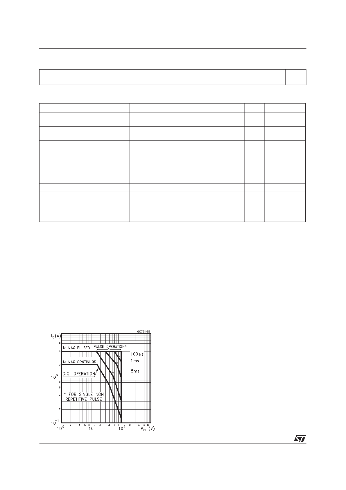
Safe Operating Areas
2/4
Page 3

TO-220 MECHANICAL DATA
BD239C
DIM.
MIN. TYP. MAX. MIN. TYP. MAX.
A 4.40 4.60 0.173 0.181
C 1.23 1.32 0.048 0.051
D 2.40 2.72 0.094 0.107
D1 1.27 0.050
E 0.49 0.70 0.019 0.027
F 0.61 0.88 0.024 0.034
F1 1.14 1.70 0.044 0.067
F2 1.14 1.70 0.044 0.067
G 4.95 5.15 0.194 0.203
G1 2.4 2.7 0.094 0.106
H2 10.0 10.40 0.393 0.409
L2 16.4 0.645
L4 13.0 14.0 0.511 0.551
L5 2.65 2.95 0.104 0.116
L6 15.25 15.75 0.600 0.620
L7 6.2 6.6 0.244 0.260
L9 3.5 3.93 0.137 0.154
DIA. 3.75 3.85 0.147 0.151
mm inch
P011C
3/4
Page 4

BD239C
Information furnished isbelieved tobe accurate andreliable. However, STMicroelectronics assumes noresponsibility for the consequences
of use of such information nor for any infringement of patents or other rights of third parties which may result from its use. No license is
granted by implication or otherwise under any patent or patent rights of STMicroelectronics. Specification mentioned in this publication are
subject tochange without notice. This publication supersedes and replaces all information previously supplied. STMicroelectronics products
are not authorized for use as critical components in life support devices or systems without express written approval of STMicroelectronics.
The ST logo is a trademark of STMicroelectronics
1999 STMicroelectronics – Printed in Italy – All Rights Reserved
STMicroelectronicsGROUP OF COMPANIES
Australia - Brazil -Canada - China - France - Germany - Italy - Japan - Korea - Malaysia - Malta - Mexico - Morocco - The Netherlands -
Singapore - Spain - Sweden - Switzerland - Taiwan - Thailand - UnitedKingdom - U.S.A.
http://www.st.com
.
4/4
 Loading...