

Page 1
LOW NOISE AUDIO AMPLIFIERS
DESCRIPTION
The BCY79 is a silicon planar epitaxial PNP
transistors in Jedec TO-18 metal case. They are
designed for use in audio driver and low-noise
input stages.
The complementaryNPN typeis the BCY59.
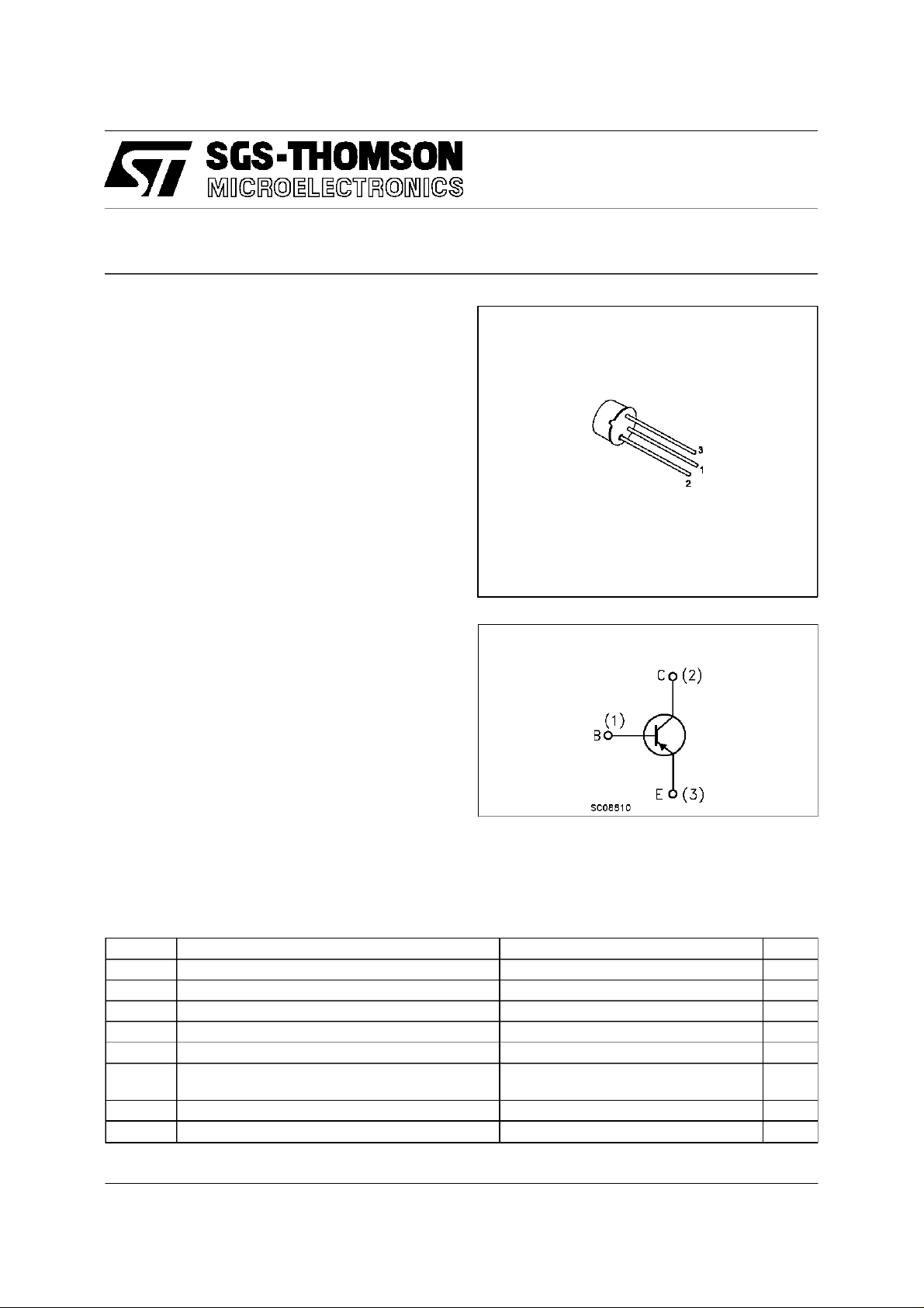
BCY79
TO-18
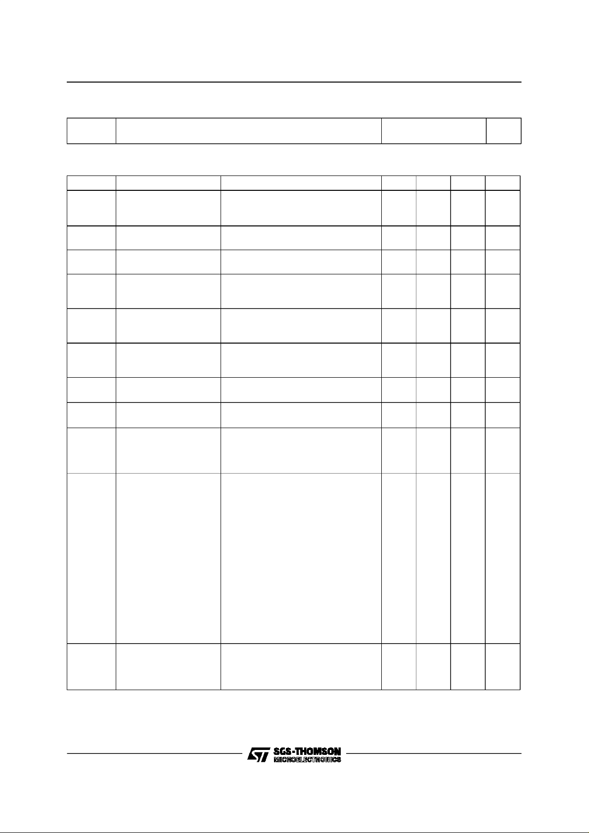
INTERNAL SCHEMATIC DIAGRAM
ABSOLUTE MAXIMUM RATINGS
Symb o l Parameter Val u e Uni t
V
V
V
I
P
T
Collector-Emitter Voltage (VBE=0) -45 V
CES
Collector-Emitter Voltage (IB=0) -45 V
CEO
Emitter-Base Voltage (IC=0) -5 V
EBO
Collect or Curr ent -200 mA
I
C
Collect or Peak Current -20 mA
CM
Total Dissipati on at T
tot
Stora ge Tem per at u re -65 to 150
stg
Max. Operating Junction Temperat u r e 150
T
j
at T
amb
case
≤ 25oC
≤ 45oC
390
1
mW
W
o
C
o
C
November 1997
1/6
Page 2
BCY79
THERMAL DATA
R
thj-case
R
thj- amb
Ther mal Resist ance Junct ion-Case Max
Thermal Resistance Junction-Ambient Max
150
450
o
C/W
o
C/W
ELECTRICAL CHARACTERISTICS (T
=25oC unlessotherwise specified)
case
Symbol Parameter Test Conditions Min. Typ. Max. Unit
I
CES
I
CEX
I
EBO
V
(BR)CES
Collector Cut-off
Current (V
BE
Collector Cut-off
Current (V
BE
Emit ter Cut - o f f Current
=0)
(I
C
∗ Co llector- Emitt er
=0)
=-2V)
=-35V
V
CE
V
=-45V
CE
=-35V T
V
CE
V
=-45V T
CE
V
=-4V -20 nA
EB
I
=-10µA-45V
C
= 150oC
amb
= 100oC-20µA
amb
-2 -20
-100
-10
Break dow n Voltage
=0)
(V
BE
V
∗ Collect or- E mitt er
(BR) CEO
I
=-2mA -45 V
C
Break dow n Voltage
=0)
(I
B
V
(BR)EBO
Emitt er-Base
I
=-1µA-5V
E
Break dow n Voltage
=0)
(I
C
V
∗ Collector-Emitt er
CE(sat)
Saturation Voltage
V
∗ Collector-Base
BE(sat )
Saturation Voltage
V
∗ Base-Emitt er O n
BE(on)
Volt age
h
∗ DC Current Gain IC=-10µAVCE=-5V
FE
IC=-10mA IB=-0.25mA
=-100mA IB=-2.5mA
I
C
IC=-10mA IB=-0.25mA
=-100mA IB=-2.5mA
I
C
IC=-10µAVCE=-5V
I
=-2mA VCE=-5V
C
=-10mA VCE=-1V
I
C
I
=-100mA VCE=-1V
C
Gr. VII
Gr. VIII
Gr. IX
=-2mA VCE=-5V
I
C
Gr. VII
Gr. VIII
Gr. IX
=-10mA VCE=-1V
I
C
Gr. VII
Gr. VIII
Gr. IX
=-100mA VCE=-1V
I
C
Gr. VII
Gr. VIII
Gr. IX
∗ Small Signal Current
h
fe
Gain
IC=-2mA VCE=-5V f=1KHz
Gr. VII
Gr. VIII
Gr. IX
∗
Pulsed: Pulse duration = 300µs, duty cycle ≤ 2%
-0.6
-0.7
-0.6
30
40
120
180
250
80
120
160
40
45
60
125
175
250
-0.12
-0.4
-0.7
-0.85
-0.55
-0.65
-0.68
-0.75
140
200
270
170
250
350
180
260
360
200
260
330
-0.25
-0.8
-0.85
-1.2
-0.75
220
310
460
400
630
250
350
500
nA
nA
µA
V
V
V
V
V
V
V
V
2/6
Page 3

BCY79
ELECTRICAL CHARACTERISTICS (continued)
Symbol Parameter Test Conditions Min. Typ. Max. Unit
f
C
EBO
C
CBO
NF Noise Figure I
h
h
h
t
t
t
t
∗
Pulsed: Pulse duration = 300µs, duty cycle ≤ 1%
Tr ansition Freque ncy IC=-10mA VCE= - 5 V f = 100 MHz 180 M Hz
T
Emitt er Base
IC=0 VEB= - 0. 5 V f = 1MHz 11 15 pF
Capacit a nc e
Collector Base
IE=0 VCB=-10V f=1MHz 4.5 7 pF
Capacit a nc e
=-0.2mA VCE=-5V
C
f=1KHz R
Input Imp edance IC=-2mA VCE=-5V f=1KHz
ie
=2KΩ
g
Gr. VII
Gr. VIII
Gr. IX
Reverse Voltage Ratio IC=-2mA VCE=-5V f=1KHz
re
Gr. VII
Gr. VIII
Gr. IX
Out put Admit t ance IC=-2mA VCE=-5V f=1KHz
oe
Gr. VII
Gr. VIII
Gr. IX
Delay Tim e VCC= -10 V
d
t
Rise Time VCC= -10 V
r
St orage T ime VCC= -10 V
s
t
Fall Time VCC= -10 V
f
Turn-on Time VCC= -10 V
on
Turn-off Time VCC= -10 V
off
=-10mA IB1=-1mA
I
C
=-100mA IB1=-10mA
I
C
I
=-10mA IB1=-1mA
C
=-100mA IB1=-10mA
I
C
=-10mA IB1=-IB2=1mA
I
C
=-100mA IB1=-IB2=10mA
I
C
=-10mA IB1=-IB2=1mA
I
C
=-100mA IB1=-IB2=10mA
I
C
=-10mA IB1=-1mA
I
C
I
=-100mA IB1=-10mA
C
=-10mA IB1=-IB2=1mA
I
C
=-100mA IB1=-IB2=10mA
I
C
26dB
2.7
3.6
4.5
1.5
2
2
18
24
30
35
5
50
50
400
250
80
200
85
55
480
450
30
50
60
150
150
800
800
KΩ
KΩ
KΩ
10
10
10
µS
µS
µS
ns
ns
ns
ns
ns
ns
ns
ns
ns
ns
ns
ns
-4
-4
-4
3/6
Page 4

BCY79
Collector-emitter SaturationVoltage. Base-emitterSaturation Voltage.
DCCurrent Gain. Normalizedh Parameters.
Noise Figurevs. Frequency. Noise Figure(f = 1 kHz).
4/6
Page 5

TO-18 MECHANICAL DATA
BCY79
DIM.
MIN. TYP. MAX. MIN. TYP. MAX.
A 12.7 0.500
B 0.49 0.019
D 5.3 0.208
E 4.9 0.193
F 5.8 0.228
G 2.54 0.100
H 1.2 0.047
I 1.16 0.045
L45
o
mm inch
o
45
G
I
H
DA
F
E
L
B
C
0016043
5/6
Page 6

BCY79
Information furnishedis believed to be accurateand reliable.However,SGS-THOMSONMicroelectronics assumes no responsability for the
consequencesof use ofsuch information nor forany infringement of patents or other rights of thirdparties which may resultsfrom its use. No
licenseis grantedby implicationor otherwise under any patent or patent rights ofSGS-THOMSONMicroelectronics. Specificationsmentioned
in this publicationare subject to change withoutnotice. This publicationsupersedes andreplacesall informationpreviously supplied.
SGS-THOMSONMicroelectronics productsare notauthorized for useas criticalcomponents inlife supportdevices or systems withoutexpress
writtenapproval of SGS-THOMSON Microelectonics.
1997 SGS-THOMSONMicroelectronics- Printedin Italy - AllRights Reserved
Australia- Brazil - Canada - China - France- Germany - Italy - Japan -Korea - Malaysia- Malta- Morocco- TheNetherlands -
Singapore- Spain- Sweden- Switzerland - Taiwan - Thailand- United Kingdom - U.S.A
SGS-THOMSONMicroelectronics GROUPOF COMPANIES
...
6/6
 Loading...