

Page 1
BCW70LT1
General Purpose
Transistors
PNP Silicon
http://onsemi.com
MAXIMUM RATINGS
Rating Symbol Value Unit
Collector–Emitter Voltage V
Emitter–Base Voltage V
Collector Current — Continuous I
THERMAL CHARACTERISTICS
Characteristic Symbol Max Unit
Total Device Dissipation FR-5 Board
TA = 25°C
Derate above 25°C
Thermal Resistance,
Junction to Ambient
Total Device Dissipation
Alumina Substrate,
Derate above 25°C
Thermal Resistance,
Junction to Ambient
Junction and Storage Temperature TJ, T
1. FR–5 = 1.0 x 0.75 x 0.062 in.
2. Alumina = 0.4 x 0.3 x 0.024 in. 99.5% alumina
(2)
TA = 25°C
(1)
CEO
EBO
C
P
R
θJA
P
R
θJA
COLLECTOR
3
–45 Vdc
–5.0 Vdc
–100 mAdc
D
D
stg
225
1.8
556 °C/W
300
2.4
417 °C/W
–55 to
+150
mW
mW/°C
mW
mW/°C
°C
1
BASE
2
EMITTER
3
1
2
SOT–23 (TO–236AB)
CASE 318
STYLE 6
DEVICE MARKING
H2x
Semiconductor Components Industries, LLC, 1999
December, 1999 – Rev. 0
x = Monthly Date Code
ORDERING INFORMATION
Device Package Shipping
BCW70LT1 SOT–23
Preferred devices are recommended choices for future use
and best overall value.
1 Publication Order Number:
3000 Units/Reel
BCW70LT1/D
Page 2

BCW70LT1
ELECTRICAL CHARACTERISTICS (T
Characteristic Symbol Min Max Unit
= 25°C unless otherwise noted)
A
OFF CHARACTERISTICS
Collector–Emitter Breakdown V oltage (IC = –2.0 mAdc, IB = 0) V
Collector–Emitter Breakdown Voltage (IC = –100 µAdc, VEB = 0) V
Emitter–Base Breakdown Voltage (IE = –10 µAdc, IC = 0) V
Collector Cutoff Current
(VCB = –20 Vdc, IE = 0)
(VCB = –20 Vdc, IE = 0, TA = 100°C)
ON CHARACTERISTICS
DC Current Gain (IC = –2.0 mAdc, VCE = –5.0 Vdc) h
Collector–Emitter Saturation Voltage (IC = –10 mAdc, IB = –0.5 mAdc) V
Base–Emitter On Voltage (IC = –2.0 mAdc, VCE = –5.0 Vdc) V
SMALL–SIGNAL CHARACTERISTICS
Output Capacitance
(IE = 0, VCB = –10 Vdc, f = 1.0 MHz)
Noise Figure
(IC = –0.2 mAdc, VCE = –5.0 Vdc, RS = 2.0 kΩ, f = 1.0 kHz, BW = 200 Hz)
(BR)CEO
(BR)CES
(BR)EBO
I
CBO
FE
CE(sat)
BE(on)
C
obo
N
F
–45 — Vdc
–50 — Vdc
–5.0 — Vdc
—
—
215 500 —
— –0.3 Vdc
–0.6 –0.75 Vdc
— 7.0 pF
— 10 dB
–100
–10
nAdc
µAdc
http://onsemi.com
2
Page 3
BCW70LT1
10
1.0
e
,
OISE
OLTA
E
n
1.0 M
R
,
SO
RCE
RESISTA
CE
O
MS
R
,
SO
RCE
RESISTA
CE
O
MS
1.0 M
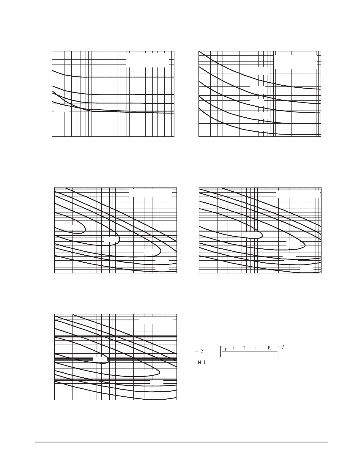
TYPICAL NOISE CHARACTERISTICS
(VCE = –5.0 Vdc, TA = 25°C)
BANDWIDTH = 1.0 Hz
7.0
V)
5.0
(
G
V
3.0
N
1.0 mA
2.0
n
1.0
10 20 50 100 200 500 1.0 k 2.0k 5.0 k 10 k
IC = 10 µA
30 µA
100 µA
300 µA
f, FREQUENCY (Hz)
RS ≈ 0
Figure 1. Noise V oltage
7.0
5.0
3.0
2.0
1.0
0.7
0.5
, NOISE CURRENT (pA)
n
I
0.3
0.2
0.1
10 20 50 100 200 500 1.0k 2.0 k 5.0 k 10 k
IC = 1.0 mA
300 µA
100 µA
30 µA
10 µA
f, FREQUENCY (Hz)
BANDWIDTH = 1.0 Hz
RS ≈∞
Figure 2. Noise Current
NOISE FIGURE CONTOURS
(VCE = –5.0 Vdc, TA = 25°C)
)
H
(
N
U
S
500 k
200 k
100 k
50 k
20 k
10 k
5.0 k
2.0 k
1.0 k
500
200
100
0.5 dB
1.0 dB
10
20 30 50 70 100 200 300 500 700 1.0k 10 20 30 50 70 100 200 300 500 700 1.0 k
IC, COLLECTOR CURRENT (µA)
BANDWIDTH = 1.0 Hz
2.0 dB
3.0 dB
5.0 dB
Figure 3. Narrow Band, 100 Hz
1.0 M
500 k
)
200 k
H
100 k
(
50 k
N
20 k
10 k
5.0 k
2.0 k
U
1.0 k
S
500
200
100
20 30 50 70 100 200 300 500 700 1.0 k
10
0.5 dB
IC, COLLECTOR CURRENT (µA)
10 Hz to 15.7 kHz
1.0 dB
2.0 dB
3.0 dB
5.0 dB
Figure 5. Wideband
500 k
200 k
100 k
50 k
20 k
10 k
5.0 k
2.0 k
1.0 k
, SOURCE RESISTANCE (OHMS)
S
500
R
200
100
0.5 dB
IC, COLLECTOR CURRENT (µA)
BANDWIDTH = 1.0 Hz
1.0 dB
2.0 dB
3.0 dB
5.0 dB
Figure 4. Narrow Band, 1.0 kHz
Noise Figure is Defined as:
2
2
2
e
)
NF+20 log
e
= Noise Voltage of the Transistor referred to the input. (Figure 3)
n
I
= Noise Current of the Transistor referred to the input.
(Figure 4)
n
K
= Boltzman’s Constant (1.38 x 10
T
= Temperature of the Source Resistance (°K)
R
= Source Resistance (Ohms)
S
10
ƪ
4KTRS)
n
4KTR
I
n
S
1ń2
R
S
ƫ
–23
j/°K)
http://onsemi.com
3
Page 4

BCW70LT1
TYPICAL STATIC CHARACTERISTICS
1.0
0.8
0.6
0.4
0.2
, COLLECTOR–EMITTER VOLTAGE (VOLTS)
CE
V
0
0.005 0.01 0.02 0.05 0.1 0.2 0.5 1.0 2.0 5.0 10 20 5.0 10 15 20 25 30 35 40
0.002
1.4
TJ = 25°C
1.2
1.0
0.8
V
0.6
V, VOLTAGE (VOLTS)
0.4
0.2
V
0
0.1 0.2 0.5
IC = 1.0 mA 10 mA 100 mA
IB, BASE CURRENT (mA)
50 mA
Figure 6. Collector Saturation Region
@ IC/IB = 10
BE(sat)
V
@ VCE = 1.0 V
BE(on)
@ IC/IB = 10
CE(sat)
1.0 2.0 5.0 10 20
IC, COLLECTOR CURRENT (mA)
TA = 25°C
50
100
100
PULSE WIDTH = 300 µs
DUTY CYCLE ≤ 2.0%
80
60
40
, COLLECTOR CURRENT (mA)
20
C
I
0
0
1.6
*APPLIES for IC/IB ≤ hFE/2
0.8
*
0
0.8
1.6
, TEMPERATURE COEFFICIENTS (mV/ C)°θ
V
qVB for V
2.4
0.1 0.2 0.5
TA = 25°C
350 µA
300 µA
VCE, COLLECTOR–EMITTER VOLTAGE (VOLTS)
IB = 400 µA
Figure 7. Collector Characteristics
qVC for V
CE(sat)
BE
1.0 2.0 5.0 10 20
IC, COLLECTOR CURRENT (mA)
25°C to 125°C
–55°C to 25°C
25°C to 125°C
250 µA
200 µA
150 µA
100 µA
50 µA
–55°C to 25°C
50
100
Figure 8. “On” Voltages
Figure 9. T emperature Coefficients
http://onsemi.com
4
Page 5

BCW70LT1
500
1000
,
TIME
ns
f,
C
RRE
T
AI
BA
I
T
RO
CT
M
1.0
TRA
SIE
T
T
ERMAL
RESISTA
CE
0
TYPICAL DYNAMIC CHARACTERISTICS
)
(
t
Hz)
(
DU
H P
D
NDW
300
200
100
7.0
5.0
500
300
200
70
50
30
20
10
td @ V
3.01.0
2.0 5.0 10
IC, COLLECTOR CURRENT (mA)
Figure 10. Turn–On Time
TJ = 25°C
VCE = 20 V
BE(off)
7.0
= 0.5 V
5.0 V
VCC = 3.0 V
IC/IB = 10
TJ = 25°C
t
r
20 30 50
70 100
700
500
300
200
100
70
t, TIME (ns)
50
30
20
10
–1.0
10
7.0
5.0
3.0
–2.0
–3.0
–5.0 –7.0
IC, COLLECTOR CURRENT (mA)
Figure 11. Turn–Off Time
–10
C
–20
ib
VCC = –3.0 V
IC/IB = 10
IB1 = I
t
s
t
f
–30
B2
TJ = 25°C
–50 –70
–100
TJ = 25°C
N —
100
–G
N
70
U
50
T
0.7 1.0 2.0 3.0 5.0 7.0 10 20 30 50
0.5
IC, COLLECTOR CURRENT (mA)
Figure 12. Current–Gain — Bandwidth Product
0.7
0.5
N
0.3
0.2
0.1
H
0.07
N
0.05
(NORMALIZED)
N
0.03
0.02
r(t)
0.01
0.01
D = 0.5
0.2
0.1
0.05
0.02
0.01
SINGLE PULSE
0.02 0.05 0.1 0.2 0.5 1.0 2.0 5.0 10 20 50 100 200 500 1.0 k 2.0 k 5.0 k 10 k 20 k
C, CAPACITANCE (pF)
2.0
1.0
0.1 0.2 0.5 1.0 2.0 5.0 10 20 500.05
P
(pk)
t, TIME (ms)
Figure 14. Thermal Response
http://onsemi.com
5
VR, REVERSE VOLTAGE (VOLTS)
Figure 13. Capacitance
FIGURE 16
t
1
t
2
DUTY CYCLE, D = t1/t
D CURVES APPLY FOR POWER
PULSE TRAIN SHOWN
READ TIME AT t1 (SEE AN–569)
Z
= r(t) • R
θ
T
J(pk)
JA(t)
– TA = P
θ
JA
(pk)
C
ob
2
Z
θ
JA(t)
10
50 k
Page 6

4
10
VCC = 30 V
3
10
I
CEO
I
CEX
, COLLECTOR CURRENT (nA)
C
I
10
10
2
10
1
10
0
10
–1
–2
–200 +20 +40 +60 +80 +100 +120 +140 +160
–4
0
TJ, JUNCTION TEMPERATURE (°C)
Figure 15. T ypical Collector Leakage Current
@ V
I
CBO
AND
BE(off)
BCW70LT1
= 3.0 V
DESIGN NOTE: USE OF THERMAL RESPONSE DATA
A train of periodical power pulses can be represented by the model
as shown in Figure 16. Using the model and the device thermal
response the normalized effective transient thermal resistance of
Figure 14 was calculated for various duty cycles.
T o find Z
steady state value R
Example:
Dissipating 2.0 watts peak under the following conditions:
Using Figure 14 at a pulse width of 1.0 ms and D = 0.2, the reading
of r(t) is 0.22.
The peak rise in junction temperature is therefore
∆T = r(t) x P
For more information, see AN–569.
, multiply the value obtained from Figure 14 by the
θJA(t)
(pk)
.
θJA
t1 = 1.0 ms, t2 = 5.0 ms (D = 0.2)
x R
= 0.22 x 2.0 x 200 = 88°C.
θJA
http://onsemi.com
6
Page 7

BCW70LT1
INFORMATION FOR USING THE SOT–23 SURFACE MOUNT PACKAGE
MINIMUM RECOMMENDED FOOTPRINT FOR SURFACE MOUNTED APPLICATIONS
Surface mount board layout is a critical portion of the
total design. The footprint for the semiconductor packages
must be the correct size to insure proper solder connection
0.037
0.95
0.035
0.9
SOT–23 POWER DISSIP ATION
The power dissipation of the SOT–23 is a function of the
pad size. This can vary from the minimum pad size for
soldering to a pad size given for maximum power
dissipation. Power dissipation for a surface mount device is
determined by T
temperature of the die, R
, the maximum rated junction
J(max)
, the thermal resistance from
θJA
the device junction to ambient, and the operating
temperature, TA. Using the values provided on the data
sheet for the SOT–23 package, PD can be calculated as
follows:
PD =
T
J(max)
R
θJA
– T
A
The values for the equation are found in the maximum
ratings table on the data sheet. Substituting these values
into the equation for an ambient temperature TA of 25°C,
one can calculate the power dissipation of the device which
in this case is 225 milliwatts.
150°C – 25°C
PD =
556°C/W
= 225 milliwatts
The 556°C/W for the SOT–23 package assumes the use
of the recommended footprint on a glass epoxy printed
circuit board to achieve a power dissipation of 225
milliwatts. There are other alternatives to achieving higher
power dissipation from the SOT–23 package. Another
alternative would be to use a ceramic substrate or an
aluminum core board such as Thermal Clad. Using a
board material such as Thermal Clad, an aluminum core
board, the power dissipation can be doubled using the same
footprint.
interface between the board and the package. With the
correct pad geometry, the packages will self align when
subjected to a solder reflow process.
0.037
0.95
0.079
2.0
0.031
0.8
inches
mm
SOT–23
SOLDERING PRECAUTIONS
The melting temperature of solder is higher than the rated
temperature of the device. When the entire device is heated
to a high temperature, failure to complete soldering within
a short time could result in device failure. Therefore, the
following items should always be observed in order to
minimize the thermal stress to which the devices are
subjected.
• Always preheat the device.
• The delta temperature between the preheat and
soldering should be 100°C or less.*
• When preheating and soldering, the temperature of the
leads and the case must not exceed the maximum
temperature ratings as shown on the data sheet. When
using infrared heating with the reflow soldering
method, the difference shall be a maximum of 10°C.
• The soldering temperature and time shall not exceed
260°C for more than 10 seconds.
• When shifting from preheating to soldering, the
maximum temperature gradient shall be 5°C or less.
• After soldering has been completed, the device should
be allowed to cool naturally for at least three minutes.
Gradual cooling should be used as the use of forced
cooling will increase the temperature gradient and
result in latent failure due to mechanical stress.
• Mechanical stress or shock should not be applied
during cooling.
* Soldering a device without preheating can cause
excessive thermal shock and stress which can result in
damage to the device.
http://onsemi.com
7
Page 8

BCW70LT1
P ACKAGE DIMENSIONS
SOT–23 (TO–236AB)
CASE 318–08
ISSUE AF
NOTES:
1. DIMENSIONING AND TOLERANCING PER ANSI
Y14.5M, 1982.
2. CONTROLLING DIMENSION: INCH.
A
L
3
1
2
S
B
GV
C
D
H
K
J
3. MAXIMUM LEAD THICKNESS INCLUDES LEAD
FINISH THICKNESS. MINIMUM LEAD THICKNESS
IS THE MINIMUM THICKNESS OF BASE
MATERIAL.
INCHES
DIMAMIN MAX MIN MAX
0.1102 0.1197 2.80 3.04
B 0.0472 0.0551 1.20 1.40
C 0.0350 0.0440 0.89 1.11
D 0.0150 0.0200 0.37 0.50
G 0.0701 0.0807 1.78 2.04
H 0.0005 0.0040 0.013 0.100
J 0.0034 0.0070 0.085 0.177
K 0.0140 0.0285 0.35 0.69
L 0.0350 0.0401 0.89 1.02
S 0.0830 0.1039 2.10 2.64
V 0.0177 0.0236 0.45 0.60
STYLE 6:
PIN 1. BASE
2. EMITTER
3. COLLECTOR
MILLIMETERS
Thermal Clad is a trademark of the Bergquist Company
ON Semiconductor and are trademarks of Semiconductor Components Industries, LLC (SCILLC). SCILLC reserves the right to make changes
without further notice to any products herein. SCILLC makes no warranty , representation or guarantee regarding the suitability of its products for any particular
purpose, nor does SCILLC assume any liability arising out of the application or use of any product or circuit, and specifically disclaims any and all liability ,
including without limitation special, consequential or incidental damages. “Typical” parameters which may be provided in SCILLC data sheets and/or
specifications can and do vary in different applications and actual performance may vary over time. All operating parameters, including “Typicals” must be
validated for each customer application by customer’s technical experts. SCILLC does not convey any license under its patent rights nor the rights of others.
SCILLC products are not designed, intended, or authorized for use as components in systems intended for surgical implant into the body, or other applications
intended to support or sustain life, or for any other application in which the failure of the SCILLC product could create a situation where personal injury or
death may occur. Should Buyer purchase or use SCILLC products for any such unintended or unauthorized application, Buyer shall indemnify and hold
SCILLC and its officers, employees, subsidiaries, affiliates, and distributors harmless against all claims, costs, damages, and expenses, and reasonable
attorney fees arising out of, directly or indirectly , any claim of personal injury or death associated with such unintended or unauthorized use, even if such claim
alleges that SCILLC was negligent regarding the design or manufacture of the part. SCILLC is an Equal Opportunity/Affirmative Action Employer .
PUBLICATION ORDERING INFORMATION
North America Literature Fulfillment:
Literature Distribution Center for ON Semiconductor
P.O. Box 5163, Denver, Colorado 80217 USA
Phone: 303–675–2175 or 800–344–3860 Toll Free USA/Canada
Fax: 303–675–2176 or 800–344–3867 Toll Free USA/Canada
Email: ONlit@hibbertco.com
N. American Technical Support: 800–282–9855 Toll Free USA/Canada
EUROPE: LDC for ON Semiconductor – European Support
German Phone: (+1) 303–308–7140 (M–F 2:30pm to 5:00pm Munich Time)
Email: ONlit–german@hibbertco.com
French Phone: (+1) 303–308–7141 (M–F 2:30pm to 5:00pm T oulouse T ime)
Email: ONlit–french@hibbertco.com
English Phone: (+1) 303–308–7142 (M–F 1:30pm to 5:00pm UK Time)
Email: ONlit@hibbertco.com
ASIA/PACIFIC: LDC for ON Semiconductor – Asia Support
Phone: 303–675–2121 (Tue–Fri 9:00am to 1:00pm, Hong Kong Time)
T oll Free from Hong Kong 800–4422–3781
Email: ONlit–asia@hibbertco.com
JAPAN: ON Semiconductor, Japan Customer Focus Center
4–32–1 Nishi–Gotanda, Shinagawa–ku, T okyo, Japan 141–8549
Phone: 81–3–5487–8345
Email: r14153@onsemi.com
Fax Response Line: 303–675–2167
800–344–3810 Toll Free USA/Canada
ON Semiconductor Website: http://onsemi.com
For additional information, please contact your local
Sales Representative.
http://onsemi.com
8
BCW70LT1/D
 Loading...