

Page 1
BCW68G
C
E
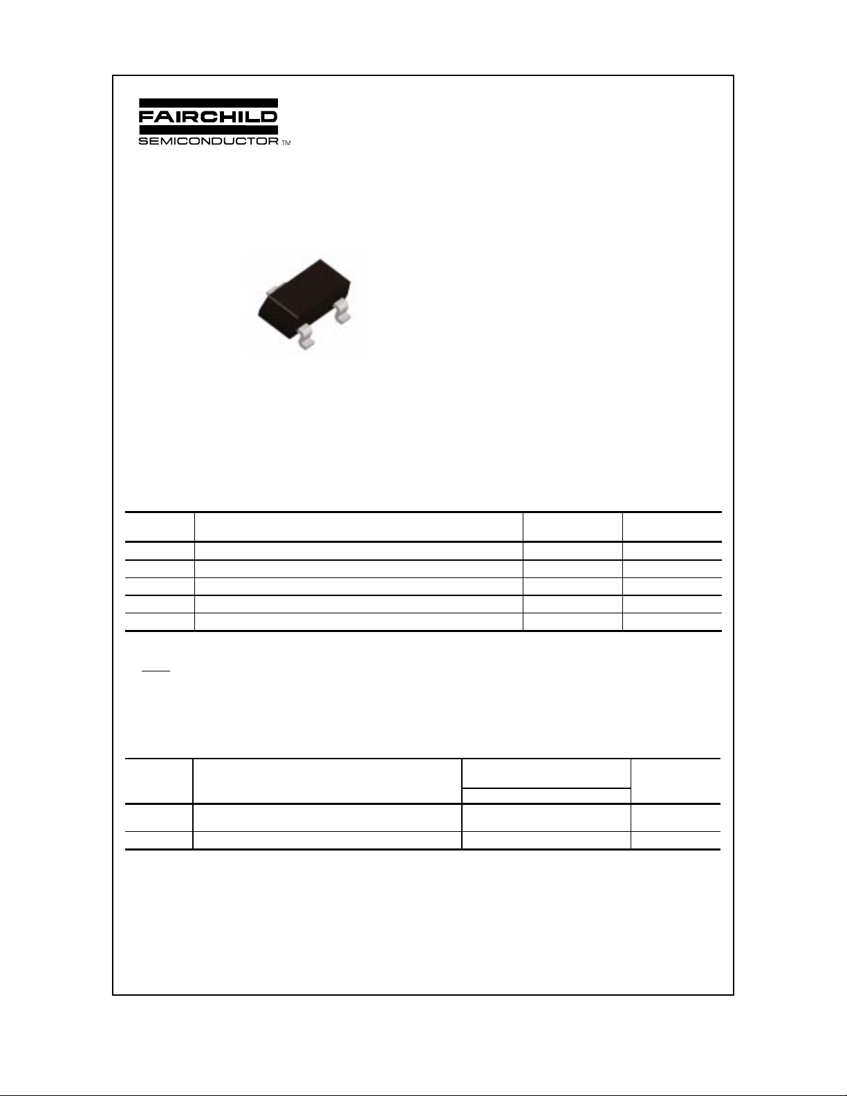
SOT-23
Mark: DG
PNP General Purpose Amplifier
This device is designed for general purpose amplifier and switching
applications at currents to 500 mA. Sourced from Process 63.
B
BCW68G
Discrete POWER & Signal
Technologies
Absolute Maximum Ratings* TA = 25°C unless otherwise noted
Symbol Parameter Value Units
V
CEO
V
CBO
V
EBO
I
C
TJ, T
stg
Collector-Emitter Voltage 45 V
Collector-Base Voltage 60 V
Emitter-Base Volta ge 5.0 V
Collector Current - Continuous 800 mA
Operating and Storage Junction Temperature Range -55 to +150
°
C
*These ratings are limiting values above which the serviceability of any semiconductor device may be impaired.
NOTES:
1) These ratings are based on a maximum junction temperature of 150 degrees C.
2) These are steady state limits. The factory should be consulted on applications involving pulsed or low duty cycle operations.
Thermal Characteristics TA = 25°C unless otherwise noted
Symbol Characteristic Max Units
*BCW68C
P
D
R
θ
JA
*Device mounted on FR-4 PCB 40 mm X 40 mm X 1.5 mm.
Total Device Dissipation
Derate above 25°C
Thermal Resistan ce, Junction to Ambien t 357
350
2.8
mW
mW/°C
C/W
°
ã 1997 Fairchild Semiconductor Corporation
Page 2
(BR)
(BR)
(BR)
(BR)
µ
PNP General Purpose Amplifier
(continued)
Electrical Characteristics TA = 25°C unless otherwise noted
Symbol Parameter Test Conditions Min Max Units
OFF CHARACTERISTICS
V
CEO
V
CES
V
CBO
V
EBO
I
CES
I
EBO
ON CHARACTERISTICS
h
FE
V
CE(
sat
V
sat
BE(
Collector-Emitter Breakdo wn Volta ge IC = 10 mA, IB = 0 45 V
Collector-Base Breakdown Voltage
Collector-Base Breakdown Voltage
Emitter-Base Breakdown Vo ltage
I
= 10 µA
C
I
= 100 µA, IE = 0
C
I
= 10 µA, IC = 0
E
Collector-Cutoff Current VCE = 45 V
V
= 45 V, TA = 150 °C
CE
Emitter-Cutoff Current VEB = 4.0 V 20 nA
DC Current Gain IC = 10 mA, VCE = 1.0 V
I
= 100 mA, VCE = 1.0 V
C
I
= 300 mA, VCE = 1.0 V
Collector-Emitter Saturation Voltage IC = 300 mA, IB = 30 mA 1.5 V
)
Base-Emitter Satura ti on Voltage IC = 500 mA, IB = 50 mA 2.0 V
)
C
120
160
60
60 V
60 V
5.0 V
20
10
400
nA
BCW68G
A
SMALL SIGNAL CHARACTERISTICS
f
T
C
obo
C
ibo
NF Noise Figure IC = 0.2 mA V, VCE = 5.0 V,
Current Gain - Bandwidth Product IC = 20 mA, VCE = 10 V,
f = 100 MHz
Ouput Capacitance VCB = 10 V, IE = 0, f = 1.0 MHz 18 pF
Input Capacitance VEB = 0.5 V, IE = 0, f = 1.0 MHz 105 pF
R
= 1.0 kΩ, f = 1.0 kHz,
S
B
= 200 Hz
W
Typical Characteristics
T y pical Pulsed Current Gain
vs Collector Current
500
400
125 °C
300
25 °C
200
100
- 40 °C
0
0.1 0.3 1 3 10 30 100 300
FE
h - TYPICAL PULSED CURRENT GAIN
I - COLLECTOR CURRENT (mA)
C
V = 5V
CE
Collector-Emi tt er Sa tu ra ti on
Voltage vs Collector Curre nt
0.5
0.4
0.3
0.2
0.1
- COLLECTOR EMITTER VOLTAGE (V)
CESAT
= 10
β
0
110100500
100 MHz
10 dB
25 °C
125 ºC
I - COLLECTOR CURRENT (mA)
C
- 40 ºC
Page 3

Typical Characteristics (continued)
BCW68G
PNP General Purpose Amplifier
(continued)
Base-Emitter Saturation
Voltage vs Collector Curre nt
1
- 40 ºC
0.8
0.6
0.4
0.2
0
BESAT
V - BASE EMITTER VOLTAGE (V)
110100500
25 °C
125 ºC
I - COLLECTOR CURRENT (mA)
C
= 10
β
Collector-Cutoff Current
vs. Ambient Temperature
100
V = 35V
CB
10
1
0.1
CBO
0.01
I - COLLECTOR CURRENT (nA)
25 50 75 100 125
T - AMBIENT TEMPERATURE ( C)
A
º
Base Emitter ON Voltage vs
Collector Current
1
0.8
0.6
0.4
0.2
0
0.1 1 10 25
BEON
V - BASE EMITTER ON VOLTAGE (V)
- 40 ºC
25 °C
125 ºC
V = 5V
CE
I - COLLECTOR CURRENT (mA)
C
Input and Output Capacitance
vs Reverse Bias Voltage
20
16
12
8
CAPACITA NCE (pF)
4
0
0.1 1 10 50
REVERSE BIAS VOLTAGE (V)
C
ib
C
ob
Power Dissipation vs
Ambient T emperature
350
300
250
200
150
100
50
D
P - POWER DISSIPATION (mW)
0
0 25 50 75 100 125 150
TEMPERATURE ( C)
SOT-23
o
Page 4

TRADEMARKS
The following are registered and unregistered trademarks Fairchild Semiconductor owns or is authorized to use and is
not intended to be an exhaustive list of all such trademarks.
ACEx™
CoolFET™
CROSSVOLT™
E2CMOS
TM
FACT™
FACT Quiet Series™
®
FAST
FASTr™
GTO™
HiSeC™
ISOPLANAR™
MICROWIRE™
POP™
PowerTrench™
QS™
Quiet Series™
SuperSOT™-3
SuperSOT™-6
SuperSOT™-8
TinyLogic™
DISCLAIMER
FAIRCHILD SEMICONDUCTOR RESERVES THE RIGHT TO MAKE CHANGES WITHOUT FURTHER
NOTICE TO ANY PRODUCTS HEREIN TO IMPROVE RELIABILITY, FUNCTION OR DESIGN. FAIRCHILD
DOES NOT ASSUME ANY LIABILITY ARISING OUT OF THE APPLICATION OR USE OF ANY PRODUCT
OR CIRCUIT DESCRIBED HEREIN; NEITHER DOES IT CONVEY ANY LICENSE UNDER ITS PATENT
RIGHTS, NOR THE RIGHTS OF OTHERS.
LIFE SUPPORT POLICY
FAIRCHILD’S PRODUCTS ARE NOT AUTHORIZED FOR USE AS CRITICAL COMPONENTS IN LIFE SUPPORT
DEVICES OR SYSTEMS WITHOUT THE EXPRESS WRITTEN APPROVAL OF FAIRCHILD SEMICONDUCTOR CORPORATION.
As used herein:
1. Life support devices or systems are devices or
systems which, (a) are intended for surgical implant into
the body, or (b) support or sustain life, or (c) whose
failure to perform when properly used in accordance
with instructions for use provided in the labeling, can be
reasonably expected to result in significant injury to the
user.
2. A critical component is any component of a life
support device or system whose failure to perform can
be reasonably expected to cause the failure of the life
support device or system, or to affect its safety or
effectiveness.
PRODUCT STATUS DEFINITIONS
Definition of Terms
Datasheet Identification Product Status Definition
Advance Information
Preliminary
No Identification Needed
Obsolete
Formative or
In Design
First Production
Full Production
Not In Production
This datasheet contains the design specifications for
product development. Specifications may change in
any manner without notice.
This datasheet contains preliminary data, and
supplementary data will be published at a later date.
Fairchild Semiconductor reserves the right to make
changes at any time without notice in order to improve
design.
This datasheet contains final specifications. Fairchild
Semiconductor reserves the right to make changes at
any time without notice in order to improve design.
This datasheet contains specifications on a product
that has been discontinued by Fairchild semiconductor.
The datasheet is printed for reference information only.
 Loading...