

Page 1
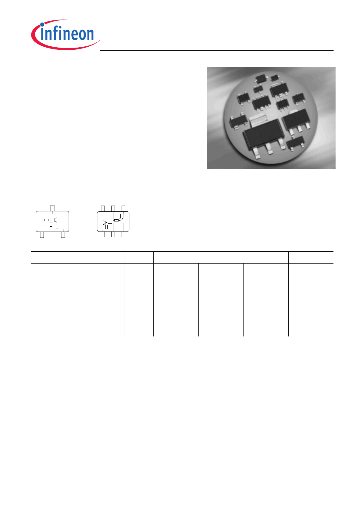
NPN Silicon Digital Transistor
• Switching in circuit, inverter, interface circuit,
drive circuit
BCR133...
• Built in bias resistor (R
= 10 kΩ, R2 = 10 kΩ)
1
• BCR133S: Two internally isolated
transistors with good matching
in one multichip package
• BCR133S: For orientation in reel see
package information below
BCR133/F/L3
BCR133S
BCR133T/W
C
3
R
1
R
2
21
EB
EHA07184
C1 B2 E2
6 54
R
2
R
TR2
1
R
TR1
1
R
2
321
C2B1E1
EHA07174
Type Marking Pin Configuration Package
BCR133
WCs
1=B
2=E
3=C
-
-
-
SOT23
BCR133F
BCR133L3
BCR133S
BCR133T
BCR133W
WCs
WC
WCs
WC
WCs
1=B
1=B
1=E1
1=B
1=B
2=E
2=E
2=B1
2=E
2=E
3=C
3=C
3=C2
3=C
3=C
-
-
4=E2
-
-
-
-
5=B2
-
-
-
-
6=C1
-
-
TSFP-3
TSLP-3-4
SOT363
SC75
SOT323
1
2006-05-04
Page 2

Maximum Ratings
)
)
j
g
BCR133...
Parameter
Symbol Value Unit
Collector-emitter voltage V
Collector-base voltage V
Input forward voltage V
Input reverse voltage V
Collector current I
Total power dissipation-
BCR133,
BCR133F,
BCR133L3,
BCR133S,
BCR133T,
BCR133W,
T
≤ 102°C
S
T
≤ 128°C
S
T
≤ 135°C
S
T
≤ 115°C
S
T
≤ 109°C
S
T
≤ 124°C
S
P
Junction temperature T
Storage temperature T
CEO
CBO
i(fwd
i(rev
C
tot
st
50 V
50
40
10
100 mA
200
250
250
250
250
250
150 °C
-65 ... 150
mW
Thermal Resistance
Parameter
Junction - soldering point1)
BCR133
BCR133F
BCR133L3
BCR133S
BCR133T
BCR133W
1
For calculation of R
please refer to Application Note Thermal Resistance
thJA
Symbol Value Unit
R
thJS
K/W
≤ 240
≤ 90
≤ 60
≤ 140
≤ 165
≤ 105
2
2006-05-04
Page 3

BCR133...
Electrical Characteristics at T
= 25°C, unless otherwise specified
Parameter
DC Characteristics
Collector-emitter breakdown voltage
I
= 100 µA, IB = 0
C
Collector-base breakdown voltage
I
= 10 µA, IE = 0
C
Collector-base cutoff current
V
= 40 V, IE = 0
CB
Emitter-base cutoff current
V
= 10 V, IC = 0
EB
DC current gain1)
I
= 5 mA, VCE = 5 V
C
Collector-emitter saturation voltage1)
I
= 10 mA, IB = 0.5 mA
C
Symbol Values Unit
min. typ. max.
V
(BR)CEO
V
(BR)CBO
I
CBO
I
EBO
h
FE
V
CEsat
50 - -
V
50 - -
- - 100 nA
- - 0.75 mA
30 - - -
- - 0.3 V
Input off voltage
I
= 100 µA, VCE = 5 V
C
Input on voltage
I
= 2 mA, VCE = 0.3 V
C
Input resistor R
V
V
i(off)
i(on)
1
Resistor ratio R1/R
AC Characteristics
Transition frequency
= 10 mA, VCE = 5 V, f = 100 MHz
I
C
Collector-base capacitance
= 10 V, f = 1 MHz
V
CB
1
Pulse test: t < 300µs; D < 2%
f
C
T
cb
0.8 - 1.5
1 - 2.5
7 10 13 kΩ
2
0.9 1 1.1 -
- 130 - MHz
- 3 - pF
3
2006-05-04
Page 4
BCR133...
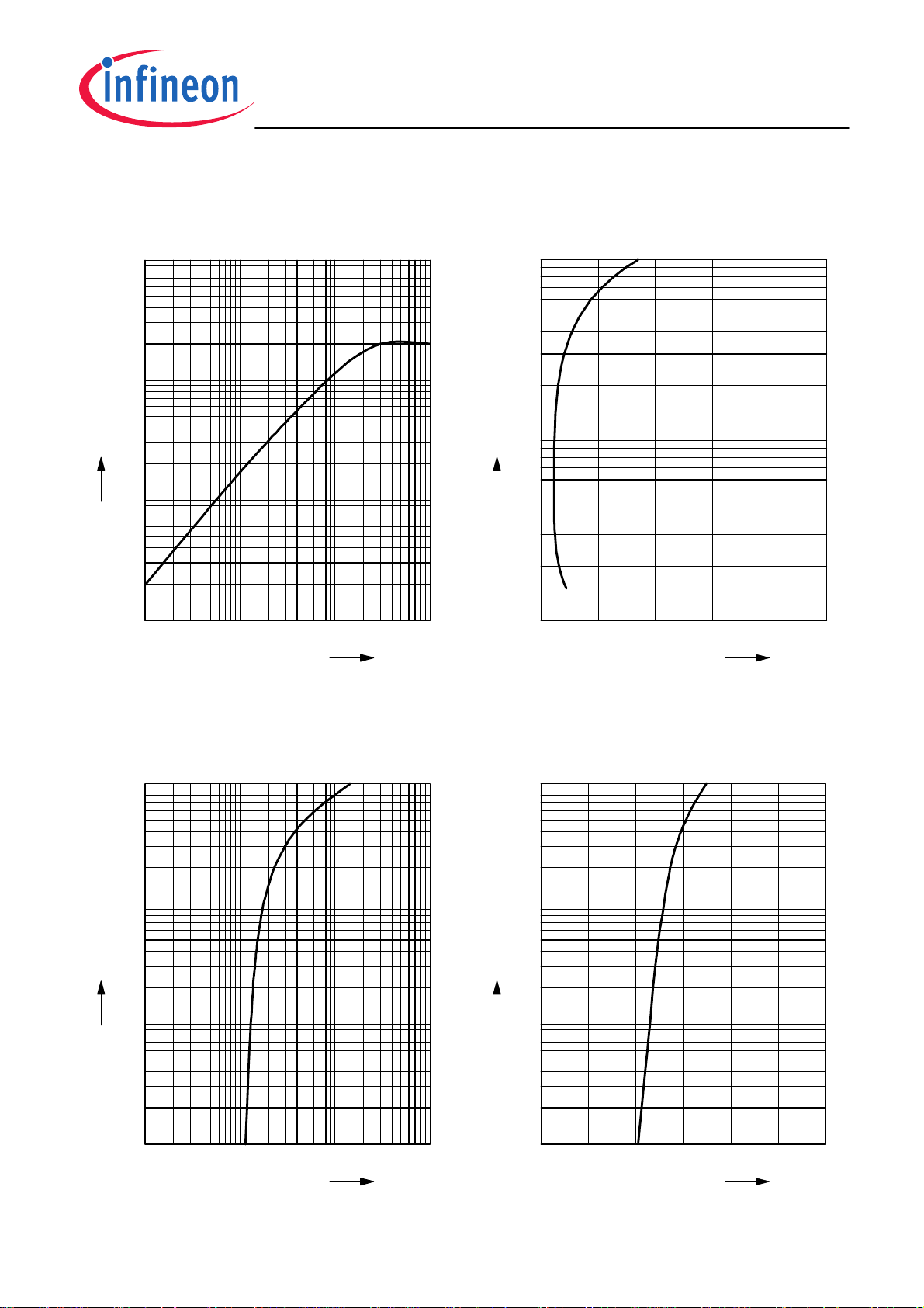
DC current gain h
= 5 V (common emitter configuration)
V
CE
3
10
-
2
10
FE
FE
= ƒ(I
)
C
h
1
10
0
10
10
-1
10
0
10
1
mA
I
Collector-emitter saturation voltage
V
2
10
C
= ƒ(I
CEsat
2
10
mA
C
I
1
10
0
10
0 0.2 0.4 0.6
), hFE = 20
C
V
V
1
CEsat
Input on Voltage Vi
= 0.3V (common emitter configuration)
V
CE
2
10
mA
1
10
C
I
0
10
-1
10
-1
10
10
(on)
0
= ƒ(IC)
10
1
Input off voltage V
= 5V (common emitter configuration)
V
CE
1
10
mA
0
10
C
I
-1
10
-2
10
0 0.5 1 1.5 2
i(on)
10
2
V
V
i(off)
= ƒ(I
)
C
V
V
3
i(off)
4
2006-05-04
Page 5
BCR133...
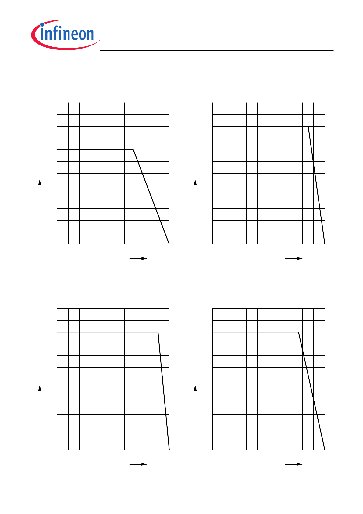
Total power dissipation P
BCR133
300
mW
250
225
200
tot
P
175
150
125
100
75
50
25
0
0 15 30 45 60 75 90 105 120
= ƒ(T
tot
)
S
Total power dissipation P
= ƒ(T
tot
)
S
BCR133F
300
mW
250
225
200
tot
P
175
150
125
100
75
50
25
0
0 15 30 45 60 75 90 105 120
T
°C
150
S
T
°C
150
S
Total power dissipation P
BCR133L3
300
mW
250
225
200
tot
P
175
150
125
100
75
50
25
0
0 15 30 45 60 75 90 105 120
= ƒ(T
tot
)
S
Total power dissipation P
= ƒ(T
tot
)
S
BCR133S
300
mW
250
225
200
tot
P
175
150
125
100
75
50
25
°C
150
T
S
0
0 15 30 45 60 75 90 105 120
T
°C
150
S
5
2006-05-04
Page 6
BCR133...
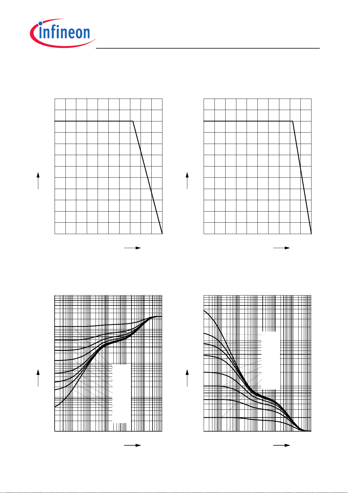
Total power dissipation P
BCR133T
300
mW
250
225
200
tot
P
175
150
125
100
75
50
25
0
0 15 30 45 60 75 90 105 120
= ƒ(T
tot
)
S
Total power dissipation P
= ƒ(T
tot
)
S
BCR133W
300
mW
250
225
200
tot
P
175
150
125
100
75
50
25
°C
150
T
S
0
0 15 30 45 60 75 90 105 120
T
°C
150
S
Permissible Pulse Load R
BCR133
3
10
K/W
2
10
thJS
R
1
10
0
10
-1
10
10
-6
10
-5
10
-4
10
-3
thJS
0.5
0.2
0.1
0.05
0.02
0.01
0.005
D = 0
= ƒ(t
-2
10
)
p
Permissible Pulse Load
P
totmax/PtotDC
= ƒ(t
)
p
BCR133
3
10
-
totDC
/ P
2
10
totmax
P
1
10
0
10
s
t
0
10
p
10
-6
10
-5
10
-4
10
D = 0
0.005
0.01
0.02
0.05
0.1
0.2
0.5
-3
10
-2
s
t
0
10
p
6
2006-05-04
Page 7

BCR133...
Permissible Puls Load R
BCR133F
2
10
K/W
1
10
thJS
R
0
10
-1
10
10
-6
10
-5
10
-4
10
thJS
D=0.5
0.2
0.1
0.05
0.02
0.01
0.005
0
-3
= ƒ (t
-2
10
)
p
Permissible Pulse Load
P
totmax/PtotDC
= ƒ(t
)
p
BCR133F
3
10
totDC
/P
2
10
totmax
P
1
10
0
10
s
t
0
10
p
10
-6
10
-5
10
D=0
0.005
0.01
0.02
0.05
0.1
0.2
0.5
-4
10
-3
10
-2
s
t
0
10
p
Permissible Puls Load R
BCR133L3
2
10
1
10
thJS
R
0
10
-1
10
-7
-6
-5
10
10
10
10
-4
thJS
10
= ƒ (t
0.5
0.2
0.1
0.05
0.02
0.01
0.005
D = 0
-3
10
)
p
Permissible Pulse Load
P
totmax/PtotDC
= ƒ(t
)
p
BCR133L3
3
10
totDC
/ P
2
10
totmax
P
1
10
0
-2
s
t
0
10
p
10
10
-7
-6
10
-5
10
10
D = 0
0.005
0.01
0.02
0.05
0.1
0.2
0.5
-4
-3
10
10
-2
s
t
0
10
p
7
2006-05-04
Page 8

BCR133...
Permissible Puls Load R
BCR133S
3
10
K/W
2
10
thJS
R
1
10
0
10
-1
10
10
-6
10
-5
10
-4
10
thJS
0.5
0.2
0.1
0.05
0.02
0.01
0.005
D = 0
-3
= ƒ (t
-2
10
)
p
Permissible Pulse Load
P
totmax/PtotDC
= ƒ(t
)
p
BCR133S
3
10
-
totDC
/ P
2
10
totmax
P
1
10
0
s
t
0
10
p
10
10
-6
10
-5
10
-4
10
D = 0
0.005
0.01
0.02
0.05
0.1
0.2
0.5
-3
10
-2
s
t
0
10
p
Permissible Puls Load R
BCR133T
3
10
K/W
2
10
thJS
R
1
10
D=0.5
0.2
0.1
0.05
10
0.02
0.01
0.005
0
-4
10
10
10
-1
0
10
-6
10
-5
thJS
-3
= ƒ (t
-2
10
)
p
Permissible Pulse Load
P
totmax/PtotDC
= ƒ(t
)
p
BCR133T
3
10
totDC
/ P
10
D=0
0.005
0.01
0.02
0.05
0.1
0.2
0.5
-4
10
-3
10
-2
s
t
0
10
p
2
10
totmax
P
1
10
0
s
t
0
10
p
10
10
-6
10
-5
8
2006-05-04
Page 9

BCR133...
Permissible Puls Load R
BCR133W
3
10
K/W
2
10
thJS
R
1
10
0
10
-1
10
10
-6
10
-5
10
-4
10
thJS
0.5
0.2
0.1
0.05
0.02
0.01
0.005
D = 0
-3
= ƒ (t
-2
10
)
p
Permissible Pulse Load
P
totmax/PtotDC
= ƒ(t
)
p
BCR133W
3
10
-
totDC
/ P
2
10
totmax
P
1
10
0
s
t
0
10
p
10
10
-6
10
-5
10
-4
10
D = 0
0.005
0.01
0.02
0.05
0.1
0.2
0.5
-3
10
-2
s
t
0
10
p
9
2006-05-04
Page 10

Package Outline
Foot Print
Package SC75
±0.2
1.6
+0.1
0.2
-0.05
A
0.2
0.10
+0.1
-0.05
0.5
M
3
1 2
0.5
0.4
0.1 MAX.
±0.2
1.6
MAX.
10˚
0.20MA
0.7
0.15
±0.1
±0.1
±0.1
0.8
MAX.
10˚
BCR133...
Marking Layout (Example)
Standard Packing
Reel ø180 mm = 3.000 Pieces/Reel
Reel ø330 mm = 10.000 Pieces/Reel
Pin 1
4
0.65
0.65
0.45
1.15
0.4
0.50.5
2005, December
Date code
BCR108T
Type code
0.2 MAX.
Pin 1
1.75
1.4
10
8
1.8
0.9
2006-05-04
Page 11

BCR133...
Date Code marking for discrete packages with
one digit (SCD80, SC79, SC75
Month 2003 2004 2005 2006 2007 2008 2009 2010 2011 2012 2013 2014
01apAPapAPapAP
02bqBQbqBQbqBQ
03crCRcrCRcrCR
04d sDSd sDSd sDS
05e t ETe t ETe t ET
06fuFUfuFUfuFU
07gvGVgvGVgvGV
08h xHXh x HXh xHX
09jyJYjyJYjyJY
10k z KZk z KZk zKZ
11l 2 L4 l 2L4 l 2L4
12n3N5n 3N5n3N5
1)
) CES-Code
1) New Marking Layout for SC75, implemented at October 2005.
.
11
2006-05-04
Page 12

Package Outline
Foot Print
Package SOT23
±0.1
2.9
12
1)
+0.1
0.4
-0.05
1.9
0.25MBC
1) Lead width can be 0.6 max. in dambar area
B
3
C
0.95
0.8
0.15 MIN.
±0.15
2.4
0.2
±0.1
1
0.1 MAX.
10˚ MAX.
0.08...0.15
0...8˚
M
A
±0.1
1.3
10˚ MAX.
A
BCR133...
Marking Layout (Example)
Standard Packing
Reel ø180 mm = 3.000 Pieces/Reel
Reel ø330 mm = 10.000 Pieces/Reel
Pin 1
0.8 1.2
EH
4
0.9
s
0.9 0.91.3
Manufacturer
2005, June
Date code (YM)
BCW66
Type code
0.2
Pin 1
3.15
2.13
12
2.65
8
1.15
2006-05-04
Page 13

Package Outline
Package SOT323
±0.2
2
0.3
+0.1
-0.05
3x
M
0.1
3
0.1 MAX.
0.1
0.9
BCR133...
±0.1
A
Foot Print
Marking Layout (Example)
12
0.650.65
0.6
0.8
0.65
0.65
1.6
±0.1
2.1
0.1 MIN.
M
0.2 A
0.15
+0.1
-0.05
±0.1
1.25
Standard Packing
Reel ø180 mm = 3.000 Pieces/Reel
Reel ø330 mm = 10.000 Pieces/Reel
Pin 1
Pin 1
2.15
Manufacturer
2005, June
Date code (YM)
BCR108W
Type code
4
8
2.3
0.2
1.1
13
2006-05-04
Page 14

Package Outline
Package SOT363
±0.2
2
0.2
+0.1
-0.05
5 4
6x
M
0.1
0.1 MAX.
0.1
0.9
BCR133...
±0.1
A
Pin 1
marking
1623
Foot Print
Marking Layout (Example)
+0.1
-0.05
±0.1
1.25
±0.1
2.1
0.1 MIN.
M
0.2 A
0.15
0.650.65
0.3
0.70.9
1.6
0.65
0.65
Small variations in positioning of
Date code, Type code and Manufacture are possible.
Pin 1 marking
Laser marking
Standard Packing
Reel ø180 mm = 3.000 Pieces/Reel
Reel ø330 mm = 10.000 Pieces/Reel
For symmetric types no defined Pin 1 orientation in reel.
4
Pin 1
marking
2.15
Manufacturer
2005, June
Date code (Year/Month)
BCR108S
Type code
0.2
8
2.3
1.1
14
2006-05-04
Page 15

Package Outline
Foot Print
Package TSFP-3
±0.05
1.2
±0.05
0.2
3
±0.05
±0.05
1.2
12
0.4
0.2
0.4
±0.05
±0.05
±0.05
0.4
0.2
0.55
±0.04
0.15
BCR133...
±0.05
0.8
10˚ MAX.
±0.05
Marking Layout (Example)
Standard Packing
Reel ø180 mm = 3.000 Pieces/Reel
Reel ø330 mm = 10.000 Pieces/Reel
Pin 1
0.45
1.05
0.4 0.4
Manufacturer
BCR847BF
Type code
Pin 1
4
1.35
0.3
1.2
1.5
15
0.2
8
0.7
2006-05-04
Page 16

Package Outline
Package TSLP-3-4
BCR133...
Top view
+0.1
0.4
0.05 MAX.
1
3
2
Pin 1
marking
±0.035
0.5
0.35
2x0.15
Bottom view
0.6
1)
3
±0.05
2
0.575
±0.05
±0.035
±0.05
1)
1
1)
±0.035
0.25
1) Dimension applies to plated terminal
2x
Foot Print
For board assembly information please refer to Infineon website "Packages"
1
0.225
0.15
0.6
0.45
0.225
R0.19
0.2
0.35
0.2
0.17
0.5
0.38
0.255
0.95
R0.1
0.2
1)
±0.035
0.4
0.315
±0.05
1
Marking Layout
Standard Packing
Reel ø180 mm = 15.000 Pieces/Reel
Stencil aperturesCopper Solder mask
BCR133L3
Type code
Pin 1 marking
Laser marking
4
1.16
8
0.5
Pin 1
marking
0.76
16
2006-05-04
Page 17

BCR133...
Edition 2006-02-01
Published by
Infineon Technologies AG
81726 München, Germany
© Infineon Technologies AG 2006.
All Rights Reserved.
Attention please!
The information given in this dokument shall in no event be regarded as a guarantee
of conditions or characteristics (“Beschaffenheitsgarantie”). With respect to any
examples or hints given herein, any typical values stated herein and/or any information
regarding the application of the device, Infineon Technologies hereby disclaims any
and all warranties and liabilities of any kind, including without limitation warranties of
non-infringement of intellectual property rights of any third party.
Information
For further information on technology, delivery terms and conditions and prices
please contact your nearest Infineon Technologies Office (www.infineon.com).
Warnings
Due to technical requirements components may contain dangerous substances.
For information on the types in question please contact your nearest
Infineon Technologies Office.
Infineon Technologies Components may only be used in life-support devices or
systems with the express written approval of Infineon Technologies, if a failure of
such components can reasonably be expected to cause the failure of that
life-support device or system, or to affect the safety or effectiveness of that
device or system.
Life support devices or systems are intended to be implanted in the human body,
or to support and/or maintain and sustain and/or protect human life. If they fail,
it is reasonable to assume that the health of the user or other persons
may be endangered.
17
2006-05-04
Page 18

 Loading...