

Page 1
NPN Silicon Digital Transistor
• Switching circuit, inverter, interface circuit,
driver circuit
• Built in bias resistor (R1=4.7kΩ, R2=4.7kΩ)
• BCR112U: Two internally isolated
transistors with good matching
in one multichip package
• BCR112U: For orientation in reel see
package information below
BCR112...
• Pb-free (RoHS compliant) package
1)
• Qualified according AEC Q101
BCR112/F
BCR112W
C
3
R
1
R
2
21
EB
EHA07184
Type Marking Pin Configuration Package
BCR112
BCR112F
BCR112W
WFs
WFs
WFs
1=B
1=B
1=B
2=E
2=E
2=E
3=C
3=C
3=C
-
-
-
-
-
-
-
-
-
SOT23
TSFP-3
SOT323
1
Pb-containing package may be available upon special request
1
2007-09-17
Page 2

Maximum Ratings
g
BCR112...
Parameter
Symbol Value Unit
Collector-emitter voltage V
Collector-base voltage V
Input forward voltage V
Input reverse voltage V
Collector current I
Total power dissipationBCR112, T
BCR112F, T
BCR112W, T
≤102°C
S
≤128°C
S
≤124°C
S
P
Junction temperature T
Storage temperature T
Thermal Resistance
Parameter
Junction - soldering point1)
BCR112
CEO
CBO
i(fwd)
i(rev)
C
tot
50 V
50
30
10
100 mA
mW
200
250
250
j
st
150 °C
-65 ... 150
Symbol Value Unit
R
thJS
K/W
≤ 240
BCR112F
BCR112W
1
For calculation of R
please refer to Application Note Thermal Resistance
thJA
≤ 90
≤ 105
-
2
2007-09-17
Page 3

Electrical Characteristics at TA = 25°C, unless otherwise specified
Parameter
Symbol Values Unit
min. typ. max.
DC Characteristics
Collector-emitter breakdown voltage
I
= 100 µA, IB = 0
C
V
(BR)CEO
50 - -
BCR112...
V
Collector-base breakdown voltage
I
= 10 µA, IE = 0
C
Collector-base cutoff current
V
= 40 V, IE = 0
CB
Emitter-base cutoff current
V
= 10 V, IC = 0
EB
DC current gain1)
I
= 5 mA, VCE = 5 V
C
Collector-emitter saturation voltage1)
I
= 10 mA, IB = 0.5 mA
C
Input off voltage
I
= 100 µA, VCE = 5 V
C
Input on voltage
I
= 2 mA, VCE = 0.3 V
C
Input resistor R
V
(BR)CBO
I
CBO
I
EBO
h
FE
V
CEsat
V
i(off)
V
i(on)
1
Resistor ratio R1/R
50 - -
- - 100 nA
- - 1.61 mA
20 - - -
- - 0.3 V
0.8 - 1.5
1 - 2.5
3.2 4.7 6.2 kΩ
2
0.9 1 1.1 -
AC Characteristics
Transition frequency
I
= 10 mA, VCE = 5 V, f = 100 MHz
C
Collector-base capacitance
V
= 10 V, f = 1 MHz
CB
1
Pulse test: t < 300µs; D < 2%
f
T
C
cb
3
- 140 - MHz
- 3 - pF
2007-09-17
Page 4
BCR112...
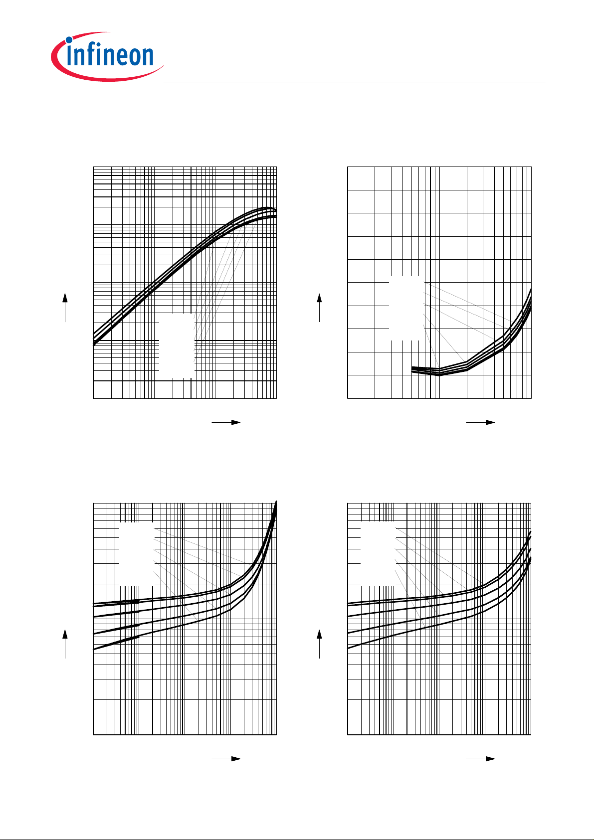
DC current gain hFE = ƒ(IC)
V
= 5 V (common emitter configuration)
CE
3
10
2
10
FE
h
1
10
-40 °C
10
-25 °C
25 °C
85 °C
125 °C
-3
10
-2
10
10
-1
0
10
-4
Collector-emitter saturation voltage
V
A
I
-1
10
C
= ƒ(IC), IC/IB = 20
CEsat
0.5
V
0.4
0.35
0.3
Vcesat
0.25
0.2
0.15
0.1
0.05
0
-3
10
-40 °C
-25 °C
25 °C
85 °C
125 °C
10
-2
A
I
-1
10
C
Input on Voltage Vi
V
= 0.3V (common emitter configuration)
CE
1
10
(on)
= ƒ(IC)
-40 °C
-25 °C
V
25 °C
85 °C
125 °C
i(on)
V
0
10
-1
10
10
-5
10
-4
10
-3
10
Input off voltage V
V
= 5V (common emitter configuration)
CE
1
10
i(off)
= ƒ(IC)
-40 °C
-25 °C
25 °C
V
85 °C
125 °C
i(off)
V
0
10
-1
-2
I
-1
A
10
C
10
10
-5
10
-4
10
-3
10
-2
I
-1
A
10
C
4
2007-09-17
Page 5

BCR112...
Total power dissipation P
BCR112
300
mW
250
225
200
tot
P
175
150
125
100
75
50
25
0
0 15 30 45 60 75 90 105 120
= ƒ(TS)
tot
T
°C
Total power dissipation P
= ƒ(TS)
tot
BCR112F
300
mW
250
225
200
tot
P
175
150
125
100
75
50
25
150
0
0 15 30 45 60 75 90 105 120
S
°C
150
T
S
Total power dissipation P
BCR112W
300
mW
250
225
200
tot
P
175
150
125
100
75
50
25
0
0 15 30 45 60 75 90 105 120
= ƒ(TS)
tot
T
°C
Permissible Pulse Load R
thJS
= ƒ(tp)
BCR112
3
10
K/W
2
10
thJS
R
1
10
0.5
0.2
0.1
0.05
10
0.02
0.01
0.005
D = 0
-3
10
-2
s
t
0
10
p
0
10
-1
10
150
10
-6
10
-5
10
-4
S
5
2007-09-17
Page 6

BCR112...
Permissible Pulse Load
P
totmax/PtotDC
= ƒ(tp)
BCR112
3
10
-
totDC
/ P
2
10
totmax
P
1
10
0
10
10
-6
10
-5
10
-4
10
D = 0
0.005
0.01
0.02
0.05
0.1
0.2
0.5
-3
10
Permissible Puls Load R
thJS
= ƒ (tp)
BCR112F
2
10
K/W
1
10
thJS
R
0
10
-1
-2
s
t
0
10
p
10
10
-6
10
-5
10
D=0.5
0.2
0.1
0.05
0.02
0.01
0.005
0
-4
10
-3
10
-2
s
t
0
10
p
Permissible Pulse Load
P
totmax/PtotDC
= ƒ(tp)
BCR112F
3
10
totDC
/P
10
totmax
P
10
10
2
1
0
10
-6
10
-5
10
D=0
0.005
0.01
0.02
0.05
0.1
0.2
0.5
-4
10
Permissible Puls Load R
thJS
= ƒ (tp)
BCR112W
3
10
K/W
2
10
thJS
R
1
10
0.5
0.2
0.1
0.05
10
0.02
0.01
0.005
D = 0
-3
10
-2
s
t
0
10
p
0
10
-1
-3
10
-2
s
t
0
10
p
10
10
-6
10
-5
10
-4
6
2007-09-17
Page 7

Permissible Pulse Load
BCR112...
P
totmax/PtotDC
BCR112W
3
10
-
totDC
/ P
2
10
totmax
P
1
10
0
10
-6
10
= ƒ(tp)
-5
10
10
D = 0
0.005
0.01
0.02
0.05
0.1
0.2
0.5
-4
10
-3
10
-2
s
t
0
10
p
7
2007-09-17
Page 8

Package Outline
Foot Print
Package SOT23
±0.1
2.9
12
1)
+0.1
0.4
-0.05
1.9
0.25MBC
1) Lead width can be 0.6 max. in dambar area
B
3
C
0.95
0.8
0.15 MIN.
±0.15
2.4
0.2
±0.1
1
0.1 MAX.
10˚ MAX.
0.08...0.15
0...8˚
M
A
±0.1
1.3
10˚ MAX.
A
BCR112...
Marking Layout (Example)
Standard Packing
Reel ø180 mm = 3.000 Pieces/Reel
Reel ø330 mm = 10.000 Pieces/Reel
Pin 1
0.8 1.2
EH
4
0.9
s
0.9 0.91.3
Manufacturer
2005, June
Date code (YM)
BCW66
Type code
0.2
Pin 1
3.15
2.13
8
2.65
8
1.15
2007-09-17
Page 9

Package Outline
Package SOT323
±0.2
2
0.3
+0.1
-0.05
3x
M
0.1
3
0.1 MAX.
0.1
0.9
BCR112...
±0.1
A
Foot Print
Marking Layout (Example)
12
0.650.65
0.6
0.8
0.65
0.65
1.6
±0.1
2.1
0.1 MIN.
M
0.2 A
0.15
+0.1
-0.05
±0.1
1.25
Standard Packing
Reel ø180 mm = 3.000 Pieces/Reel
Reel ø330 mm = 10.000 Pieces/Reel
Pin 1
Pin 1
2.15
Manufacturer
2005, June
Date code (YM)
BCR108W
Type code
4
8
2.3
0.2
1.1
9
2007-09-17
Page 10

Package Outline
Foot Print
Package TSFP-3
±0.05
1.2
±0.05
0.2
3
±0.05
±0.05
1.2
12
0.4
0.2
0.4
±0.05
±0.05
±0.05
0.4
0.2
0.55
±0.04
0.15
BCR112...
±0.05
0.8
10˚ MAX.
±0.05
Marking Layout (Example)
Standard Packing
Reel ø180 mm = 3.000 Pieces/Reel
Reel ø330 mm = 10.000 Pieces/Reel
Pin 1
0.45
1.05
0.4 0.4
Manufacturer
BCR847BF
Type code
Pin 1
4
1.35
0.3
1.2
1.5
10
0.2
8
0.7
2007-09-17
Page 11

BCR112...
Edition 2006-02-01
Published by
Infineon Technologies AG
81726 München, Germany
© Infineon Technologies AG 2007.
All Rights Reserved.
Attention please!
The information given in this dokument shall in no event be regarded as a guarantee
of conditions or characteristics (“Beschaffenheitsgarantie”). With respect to any
examples or hints given herein, any typical values stated herein and/or any information
regarding the application of the device, Infineon Technologies hereby disclaims any
and all warranties and liabilities of any kind, including without limitation warranties of
non-infringement of intellectual property rights of any third party.
Information
For further information on technology, delivery terms and conditions and prices
please contact your nearest Infineon Technologies Office (www.infineon.com).
Warnings
Due to technical requirements components may contain dangerous substances.
For information on the types in question please contact your nearest
Infineon Technologies Office.
Infineon Technologies Components may only be used in life-support devices or
systems with the express written approval of Infineon Technologies, if a failure of
such components can reasonably be expected to cause the failure of that
life-support device or system, or to affect the safety or effectiveness of that
device or system.
Life support devices or systems are intended to be implanted in the human body,
or to support and/or maintain and sustain and/or protect human life. If they fail,
it is reasonable to assume that the health of the user or other persons
may be endangered.
11
2007-09-17
Page 12

 Loading...