

Page 1
CYStech Electronics Corp.
PNPN Epitaxial Planar SCR
Spec. No. : C700A3
Issued Date : 2008.02.22
Revised Date :2012.10.16
Page No. : 1/6
BCR1002A3
Descriptions
The BCR1002A3 is designed for high volume consumer applications such as temperature, light, and speed
control; process and remote control, and warning systems where reliability of operation is important.
Features
• Practical level triggering and holding characteristics
• On state current rating of 0.35A
• Sensitive gate allows triggering by microcontrollers and other logic circuits
• Pb-free package
RMS
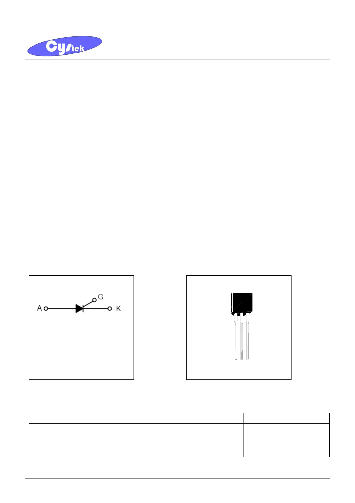
Symbol Outline
BCR1002A3
G:Gate
A:Anode
K:Cathode
Ordering Information
Device Package Shipping
BCR1002A3-0-TB-G
BCR1002A3-0-BK-G
(Pb-free lead plating and halogen-free package)
(Pb-free lead plating and halogen-free package)
TO-92
TO-92
TO-92
K G A
2000 pcs / tape & box
1000 pcs / bag; 10 bags/box,
10 boxes/carton
BCR1002A3 CYStek Product Specification
Page 2
CYStech Electronics Corp.
Absolute Maximum Ratings (TJ=25°C)
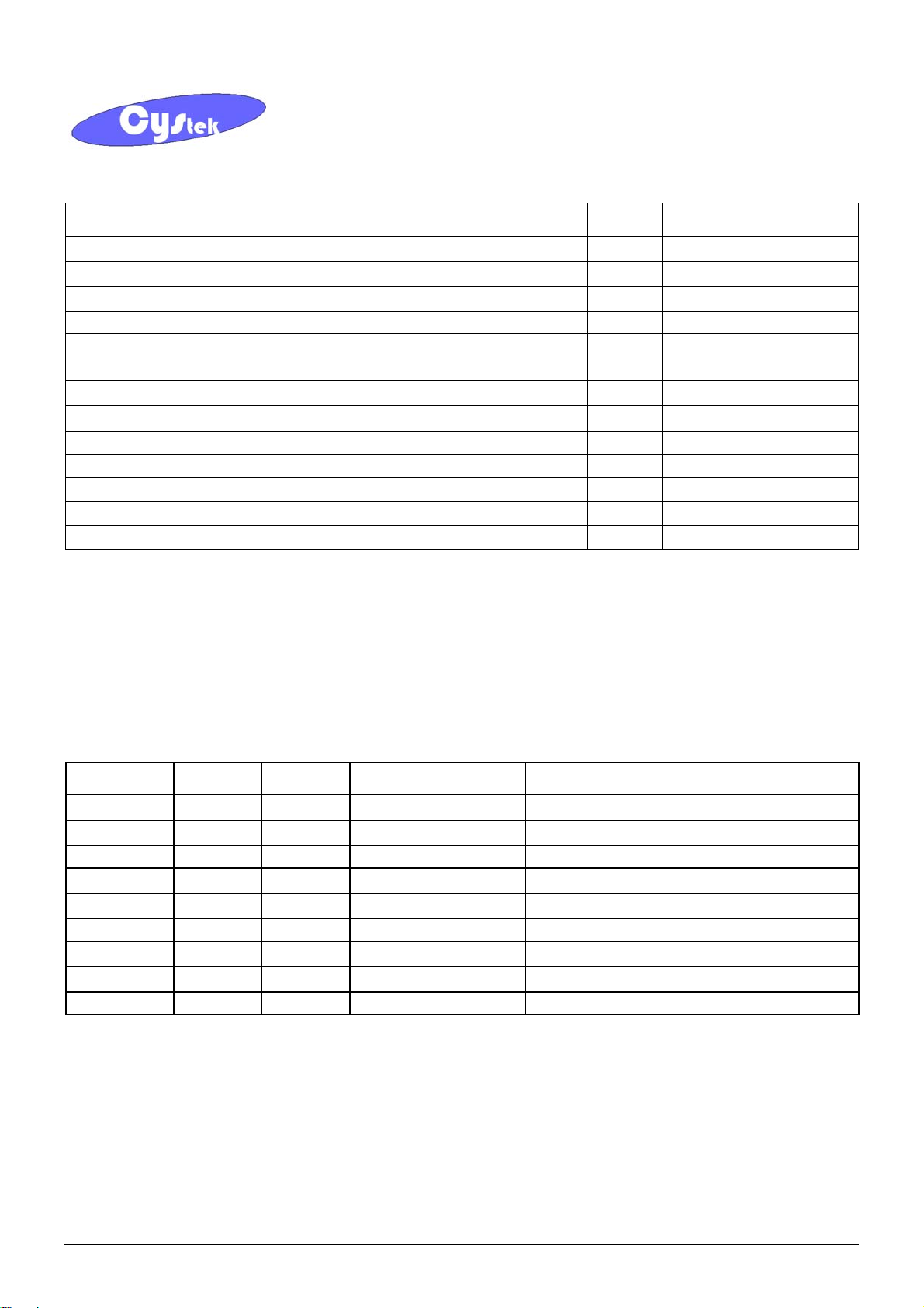
Parameter Symbol Limits Unit
Spec. No. : C700A3
Issued Date : 2008.02.22
Revised Date :2012.10.16
Page No. : 2/6
Peak Repetitive Off-State Voltage @TJ=-40℃ to 125℃, RGK=1KΩ
On-State Current @TC=80℃
Average On-State Current @ TC=80℃
VDRM 140 V
IT(RMS) 350 mA
IT(AV) 220 mA
Peak Non-repetitive Surge Current, half cycle, sine wave, 60Hz ITSM 4 A
Circuit Fusing Consideration (t=8.3ms) I²t 0.2 A²s
Reverse Peak Gate Voltage @TA=25℃, Pulse Width≤1μs
Forward Peak Gate Current @TA=25℃, Pulse Width≤1μs
Forward Average Gate Power @ TA=25℃, t=8.3ms
Thermal Resistance, Junction to Ambient RθJA 200
Thermal Resistance, Junction to Case RθJC 75
Junction Temperature Tj -40~+125
Storage Temperature Tstg -40~+150
Lead Solder Temperature(<1/16” from case, 10secs max) TL 260
Note : Stress exceeding maximum ratings may damage the device. Maximum ratings are stress ratings only. Functional
operation above the recommended operating conditions is not implied. Extended exposure to stresses above the
recommended operating conditions may affect device reliability.
V
DRM can be applied on a continuous basis. Ratings apply for zero or negative gate voltage; however , positive gate
voltage shall not be applied concurrent with negative potential on the anode. Blocking voltage shall not be tested with
a constant current source such that the voltage ratings of the device are exceeded.
VGRM 8 V
IGM 500 mA
PG(AV) 100 mW
°C/W
°C/W
°C
°C
°C
Characteristics
(Ta=25°C)
Symbol Min. Typ. Max. Unit Test Conditions
I
- - 100 μA
DRM
I
- - 10 μA
DRM
VD=140V, RGK=1KΩ, TC=125℃
VD=140V, RGK=1KΩ, TC=25℃
*VTM - - 1.5 V ITM=200mA
IGT - - 100
IH - - 5
μA
mA
VD=7V, RL=100Ω
VD=7V, RGK=1KΩ
IL - - 6 mA VD=7V, IG=200μA
VGT - - 0.8 V
dV/dt 25 - - V/μs
VD=7V, RL=100Ω
VD=35V, RGK=1KΩ
dI/dt 30 - - A/μs IG=10mA, dIG/dt=100mA/μs, PW=10μs
*Pulse Test: Pulse Width ≤300μs, Duty Cycle≤2%
BCR1002A3 CYStek Product Specification
Page 3
CYStech Electronics Corp.
Typical Characteristics
Spec. No. : C700A3
Issued Date : 2008.02.22
Revised Date :2012.10.16
Page No. : 3/6
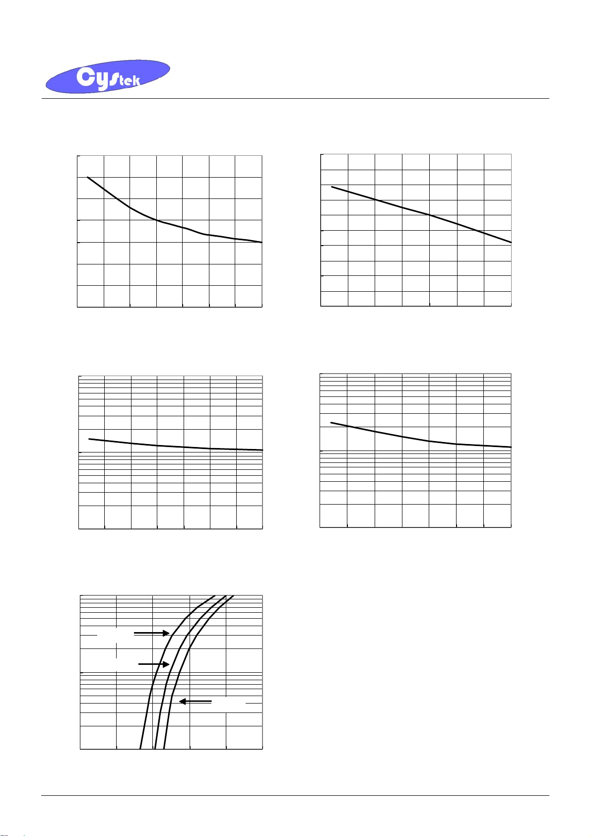
Gate Trigger Current vs Junction Temperature
70
60
A)
μ
(
GT
50
40
30
20
Gate Trigger Current---I
10
0
-50 -25 0 25 50 75 100 125
JunctionTemperature---T
(℃)
J
Holding Current vs Junction Temperature
10
(mA)
H
Gate Trigger Voltage vs Junction Temperature
1
0.9
(V)
0.8
GT
0.7
0.6
0.5
0.4
0.3
0.2
Gate Trigger Voltage---V
0.1
0
-50-250 255075100125
Junction Temperature---T
(°C)
J
Latching Current vs Junction Temperature
1000
A)
μ
(
L
1
Holding Current---I
0.1
-50 -25 0 25 50 75 100 125
Junction Temperature---T
(°C)
J
On-state Characteristics
1000
(mA)
T
100
Instantaneous On-state Current---I
TJ=125°C
TJ=25°C
TJ=-40°C
100
Latching Current---I
10
-50 -25 0 25 50 75 100 125
Junction Temperature---T
(°C)
J
10
00.40.81.21.62
Instantaneous On-state Voltage---V
T
(V)
BCR1002A3 CYStek Product Specification
Page 4

CYStech Electronics Corp.
TO-92 Taping Outline
H2H2
Spec. No. : C700A3
Issued Date : 2008.02.22
Revised Date :2012.10.16
Page No. : 4/6
H2AH2A
D2
A
H3
H4
L
L1
H1
T2
T
T1
P1
F1F2
P
D1
P2
D
DIM Item
A Component body height 4.33 4.83
D Tape Feed Diameter 3.80 4.20
D1 Lead Diameter
D2 Component Body Diameter 4.33 4.83
F1,F2 Component Lead Pitch 2.40 2.90
F1,F2 F1-F2 -
H Height Of Seating Plane 15.50 16.50
H1 Feed Hole Location 8.50 9.50
H2 Front To Rear Deflection - 1
H2A Deflection Left Or Right - 1
H3 Component Height - 27
H4 Feed Hole To Bottom Of Component - 21
L Lead Length After Component Removal - 11
L1 Lead Wire Enclosure 2.50 -
P Feed Hole Pitch 12.50 12.90
P1 Center Of Seating Plane Location 5.95 6.75
P2 4 Feed Hole Pitch 50.30 51.30
T Over All Tape Thickness - 0.55
T1 Total Taped Package Thickness - 1.42
T2 Carrier Tape Thickness 0.36 0.68
W Tape Width 17.50 19.00
W1 Adhesive Tape Width 5.00 7.00
- 20 pcs Pitch 253 255
Millimeters
Min. Max.
0.36 0.53
H
W1
W
±0.3
BCR1002A3 CYStek Product Specification
Page 5

CYStech Electronics Corp.
Recommended wave soldering condition
Product Peak Temperature Soldering Time
Spec. No. : C700A3
Issued Date : 2008.02.22
Revised Date :2012.10.16
Page No. : 5/6
Pb-free devices
260 +0/-5 °C
Recommended temperature profile for IR reflow
5 +1/-1 seconds
Profile feature Sn-Pb eutectic Assembly
Average ramp-up rate
(Tsmax to Tp)
Preheat
−Temperature Min(T
−Temperature Max(TS max)
−Time(ts min to ts max)
Time maintained above:
−Temperature (TL)
− Time (tL)
Peak Temperature(TP)
Time within 5°C of actual peak
temperature(tp)
Ramp down rate
Time 25 °C to peak temperature
Note : All temperatures refer to topside of the package, measured on the package body surface.
S min)
3°C/second max. 3°C/second max.
100°C
150°C
60-120 seconds
183°C
240 +0/-5 °C 260 +0/-5 °C
10-30 seconds 20-40 seconds
6°C/second max. 6°C/second max.
6 minutes max. 8 minutes max.
Pb-free Assembly
150°C
200°C
60-180 seconds
217°C
60-150 seconds 60-150 seconds
BCR1002A3 CYStek Product Specification
Page 6

g
TO-92 Dimension
CYStech Electronics Corp.
Spec. No. : C700A3
Issued Date : 2008.02.22
Revised Date :2012.10.16
Page No. : 6/6
A
Product Name
α2
Marking:
R1002
F
DIM
B
31
2
α3
Date Code: Year+Month
Year: 4→2004, 5→2005
Month: 1→1, 2→2, ‧‧‧,
C
H
I
D
9→9, A→10, B→11, C→12
G
α1
E
Inches Millimeters Inches Millimeters
Min. Max. Min. Max.
DIM
Style: Pin 1.Cathode 2.Gate 3.Anode
3-Lead TO-92 Plastic Package
CYStek Packa
Min. Max. Min. Max.
□□
e Code: A3
*: Typical
A 0.1704 0.1902 4.33 4.83 G 0.0142 0.0220 0.36 0.56
B 0.1704 0.1902 4.33 4.83 H - *0.1000 - *2.54
C 0.5000 - 12.70 - I - *0.0500 - *1.27
D 0.0142 0.0220 0.36 0.56
E - *0.0500 - *1.27
F 0.1323 0.1480 3.36 3.76
Notes: 1.Controlling dimension: millimeters.
2.Maximum lead thickness includes lead finish thickness, and minimum lead thickness is the minimum thickness of base material.
3.If there is any question with packing specification or packing method, please contact your local CYStek sales office.
Material:
• Lead: Pure tin plated.
• Mold Compound: Epoxy resin family, flammability solid burning class: UL94V-0.
α1
α2
α3
-
-
-
*5°
*2°
*2°
-
-
-
Important Notice:
• All rights are reserved. Reproduction in whole or in part is prohibited without the prior written approval of CYStek.
• CYStek reserves the right to make changes to its products without notice.
• CYStek semiconductor products are not warranted to be suitable for use in Life-Support Applications, or systems.
• CYStek assumes no liability for any consequence of customer product design, infringement of patents, or application assistance.
*5°
*2°
*2°
BCR1002A3 CYStek Product Specification
Page 7

 Loading...