

BCP69
PNP General Purpose Amplifier
• This device is designed for general purpose medium power amplifiers
and switches requiring collector currents to 1.0A.
• Sourced from Process 77.
January 2007
4
3
2
1
SOT-223
1. Base 2. Collector 3. Emitter
BCP69 PNP General Purpose Amplifier
Absolute Maximum Ratings* T
=25°C unless otherwise noted
a
Symbol Parameter Value Units
V
CEO
V
CBO
V
EBO
I
C
T
J
T
STG
* These ratings are limiting values above which the serviceability of any semiconductor device may be impaired.
NOTES:
1) These ratings are based on a maximum junction temperature of 150°C.
2) These are steady state limits. The factory should be consulted on applications involving pulsed or low duty cycle operations.
Thermal Characteristics* T
Symbol Parameter Value
P
D
R
θJA
* Device mounted on FR-4 PCB 36mm × 18mm × 1.5mm; mounting pad for the collector lead min. 6cm
Electrical Characteristics* T
Collector-Emitter Voltage -20 V
Collector-Base Voltage -30 V
Emitter-Base Voltage -5.0 V
Collector Current - Continuous -1.5 A
Junction Temperature 150 °C
Storage Temperature Range - 55 ~ +150 °C
=25°C unless otherwise noted
a
Units
Total Device Dissipation
Derate above 25°C
Thermal Resistance, Junction to Ambient 125 °C/W
2
= 25°C unless otherwise noted
a
1.0
8.0
W
mW/°C
Symbol Parameter Test Conditions Min. Typ. Max. Units
BV
CEO
BV
CBO
BV
EBO
I
CBO
I
EBO
h
FE
V
CE(sat)
V
BE(on)
C
cb
h
fe
* Pulse Test: Pulse Width ≤ 300µs, Duty Cycle ≤ 2.0%
Collector-Emitter Breakdown Voltage IC = -10mA, IB = 0 -20 V
Collector-Base Breakdown Voltage IC = -1.0mA, IE = 0 -30 V
Emitter-Base Breakdown Voltage IE = -100µA, IC = 0 -5.0 V
Collector-Base Cutoff Current VCB = -25V, IE = 0
VCB = -25V, IE = 0, Tj = 150oC
-100
-10
nA
uA
Emitter-Base Cutoff Current VEB = -5.0V, IC = 0 -100 nA
DC Current Gain IC = -5mA, VCE = -1.0V
IC = -500mA, VCE = -1.0V
IC = -1.0A, VCE = -1.0V
50
85
60
375
Collector-Emitter Saturation Voltage IC = -1.0A, IB = -100mA -0.5 V
Base-Emitter On Voltage IC = -1.0A, VCE = -1.0V -1.0 V
Collector-Base Capacitance VCB = -10V, IE = 0, f = 1.0MHz 30 pF
Small-Signal Current Gain IC = -50mA, VCE = -10V, f = 20MHz 2.5
©2007 Fairchild Semiconductor Corporation 1 www.fairchildsemi.com
BCP69 Rev. B
0
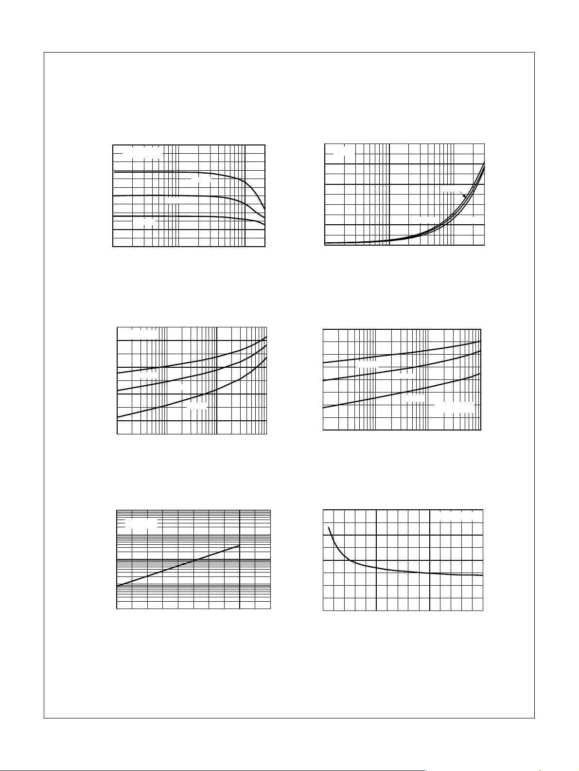
Typical Performance Characteristics
BCP69 PNP General Purpose Amplifier
Typical Puls ed Curr ent Gain
vs Collector Current
300
V = 5.0V
CE
125 °C
25 °C
50
0
- 40 °C
0.01 0.1 1 2
I - COLLEC TOR CU RRE NT (A)
C
h - TYPICAL PULSED CURRENT GAIN
250
200
150
100
FE
Bas e-Emitter Sat u ra tion
Voltage vs Collector Current
= 10
β
1
0.8
0.6
0.4
BESAT
V - BASE-EMITTER VOLTAGE (V)
- 40 °C
25 °C
125 °C
1 10 100 1000
I - COLLECTOR CURRE NT (mA )
C
Col le cto r-Emitter Satu r ati on
V o ltage v s C o lle cto r Current
1
= 10
β
0.8
0.6
0.4
0.2
0
0.01 0.1 1 3
CESAT
V - COL LECTO R-EMITTER VOLTA G E (V)
I - COLLECTOR CURRENT (A)
C
- 40 °C
25 °C
125 °C
Base-Emitter ON V oltage vs
Collector Current
1
0.8
0.6
0.4
0.2
BE(ON)
110100100
V - BASE-EMITTER ON VOLTAGE (V)
- 40 °C
25°C
125°C
I - COLLECTOR CURRENT (mA)
C
V = 5.0 V
CE
BCP69 Rev. B
Collector-Cutoff Current
vs Ambient Tem per ature
100
V = 20V
CB
10
1
0.1
CBO
I - COLLECTOR CURR ENT (nA)
25 50 75 100 125 150
T - AM BI E N T TE MP E RATU R E ( C)
A
°
Collector-Base Capacitance
vs Collector-Base Voltage
40
30
20
10
0
0102030
OBO
C - COLLECTOR-BASE CAPACITANCE (pF)
V - COLLECTOR-BASE VOLTA GE ( V )
CB
2 www.fairchildsemi.com
f = 1.0 MHz

Typical Performance Characteristics
0
BCP69 PNP General Purpose Amplifier
Gain Bandwidth Product
vs Collecto r Curr en t
250
V = 10V
CE
200
150
100
50
0
T
1 10 100 1000
f - GAIN BANDWID T H PRO DU CT (M Hz)
I - COLLECTOR CURRENT (mA)
C
Power Dissipation vs
Power Dissipation vs
Amb ient Temp erature
700
Amb ient Temp erature
1.5
600
500
1.0
400
300
0.5
200
100
D
[W], POWER DISSIPATION
P - POWER DISS I PATION (mW)
C
P
0.0
0
0 255075100125150
0 25 50 75 100 125 15
Ta[oC], AMBIENT TEMPERATURE
TEMPER ATURE ( C)
TO-92
o
BCP69 Rev. B
3 www.fairchildsemi.com
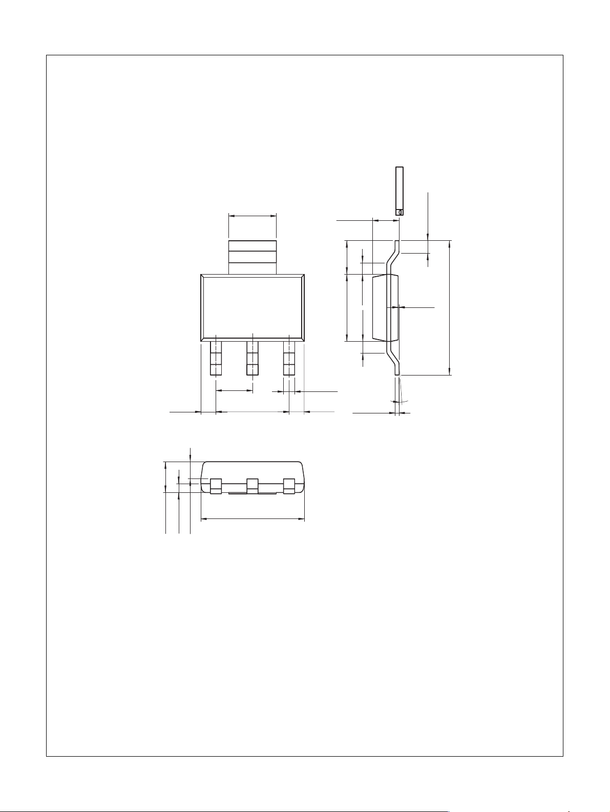
Mechanical Dimensions
1
(
3.00
SOT-223
±0.10
MAX1.80
±0.20
1.75
±0.20
0.08MAX
+0.04
0.06
–0.02
BCP69 PNP General Purpose Amplifier
±0.20
0.65
±0.30
2.30 TYP
(0.95) (0.95)
±0.20
.60
0.46)(0.89)
4.60
6.50
±0.25
±0.20
0.70
±0.10
3.50
(0.60) (0.60)
0.25
+0.10
–0.05
7.00
0°~10°
Dimensions in Millimeters
4 www.fairchildsemi.com
BCP69 Rev. B

FAIRCHILD SEMICONDUCTOR TRADEMARKS
The following are registered and unregistered trademarks Fairchild Semiconductor owns or is authorized to use and is not intended to
be an exhaustive list of all such trademarks.
ACEx™
ActiveArray™
Bottomless™
Build it Now™
CoolFET™
CROSSVOLT™
DOME™
EcoSPARK™
2
E
CMOS™
EnSigna™
®
FACT
®
FAST
FASTr™
FPS™
FRFET™
FACT Quiet Series™
GlobalOptoisolator™
GTO™
HiSeC™
2
I
C™
i-Lo™
ImpliedDisconnect™
IntelliMAX™
ISOPLANAR™
LittleFET™
MICROCOUPLER™
MicroFET™
MicroPak™
MICROWIRE™
MSX™
MSXPro™
Across the board. Around the world.™
The Power Franchise
®
OCX™
OCXPro™
OPTOLOGIC
®
OPTOPLANAR™
PACMAN™
POP™
Power247™
PowerEdge™
PowerSaver™
PowerTrench
QFET
®
®
QS™
QT Optoelectronics™
Quiet Series™
RapidConfigure™
RapidConnect™
µSerDes™
ScalarPump™
SILENT SWITCHER
SMART START™
SPM™
Stealth™
SuperFET™
SuperSOT™-3
SuperSOT™-6
SuperSOT™-8
SyncFET™
TCM™
TinyBoost™
TinyBuck™
TinyPWM™
TinyPower™
TinyLogic
®
TINYOPTO™
TruTranslation™
®
UHC
®
UniFET™
VCX™
Wire™
Programmable Active Droop™
BCP69 PNP General Purpose Amplifier
BCP69 PNP General Purpose Amplifier
DISCLAIMER
FAIRCHILD SEMICONDUCTOR RESERVES THE RIGHT TO MAKE CHANGES WITHOUT FURTHER NOTICE TO ANY PRODUCTS HEREIN TO
IMPROVE RELIABILITY, FUNCTION OR DESIGN. FAIRCHILD DOES NOT ASSUME ANY LIABILITY ARISING OUT OF THE APPLICATION OR USE
OF ANY PRODUCT OR CIRCUIT DESCRIBED HEREIN;NEITHER DOES IT CONVEY ANY LICENSE UNDER ITS PATENT RIGHTS, NOR THE
RIGHTS OF OTHERS. THESE SPECIFICATIONS DO NOT EXPAND THE TERMS OF FAIRCHILD’S WORLDWIDE TERMS AND CONDITIONS, SPECIFICALLY THE WARRANTY THEREIN, WHICH COVERS THESE PRODUCTS.
LIFE SUPPORT POLICY
FAIRCHILD’S PRODUCTS ARE NOT AUTHORIZED FOR USE AS CRITICAL COMPONENTS IN LIFE SUPPORT DEVICES OR SYSTEMS WITHOUT
THE EXPRESS WRITTEN APPROVAL OF FAIRCHILD SEMICONDUCTOR CORPORATION.
As used herein:
1. Life support devices or systems are devices or systems which, (a) are
intended for surgical implant into the body, or (b) support or sustain life, or
(c) whose failure to perform when properly used in accordance with
instructions for use provided in the labeling, can be reasonably expected
to result in significant injury to the user.
2. A critical component is any component of a li fe support device or system
whose failure to perform can be reasonably expected to cause the failure
of the life support device or system, or to affect its safety or eff ectiveness.
PRODUCT STATUS DEFINITIONS
Definition of Terms
Datasheet Identification Product Status Definition
Advance Information Formative or In Design This datasheet contains the design specifications for
Preliminary First Production This datasheet contains preliminary data, and
No Identification Needed Full Production This datasheet contains final specifications. Fairchild
product development. Specifications may change in
any manner without notice.
supplementary data will be published at a later date.
Fairchild Semiconductor reserves the right to make
changes at any time without notice in order to improve
design.
Semiconductor reserves the right to make changes at
any time without notice in order to improve design.
Obsolete Not In Production This datasheet contains specifications on a produ ct
BCP69 Rev. B
that has been discontinued by Fairchild semiconductor.
The datasheet is printed for reference information only.
5 www.fairchildsemi.com
Rev. I22
 Loading...