

Page 1
NPN Silicon AF Transistors BCP 54
... BCP 56
● For AF driver and output stages
● High collector current
● Low collector-emitter saturation voltage
● Complementary types: BCP 51 … BCP 53 (PNP)
Type Marking
BCP 54
BCP 54-10
BCP 54-16
BCP 55
BCP 55-10
BCP 55-16
BCP 56
BCP 56-10
BCP 56-16
BCP 54
BCP 54-10
BCP 54-16
BCP 55
BCP 55-10
BCP 55-16
BCP 56
BCP 56-10
BCP 56-16
Ordering Code
(tape and reel)
Q62702-C2117
Q62702-C2119
Q62702-C2120
Q62702-C2148
Q62702-C2122
Q62702-C2123
Q62702-C2149
Q62702-C2125
Q62702-C2106
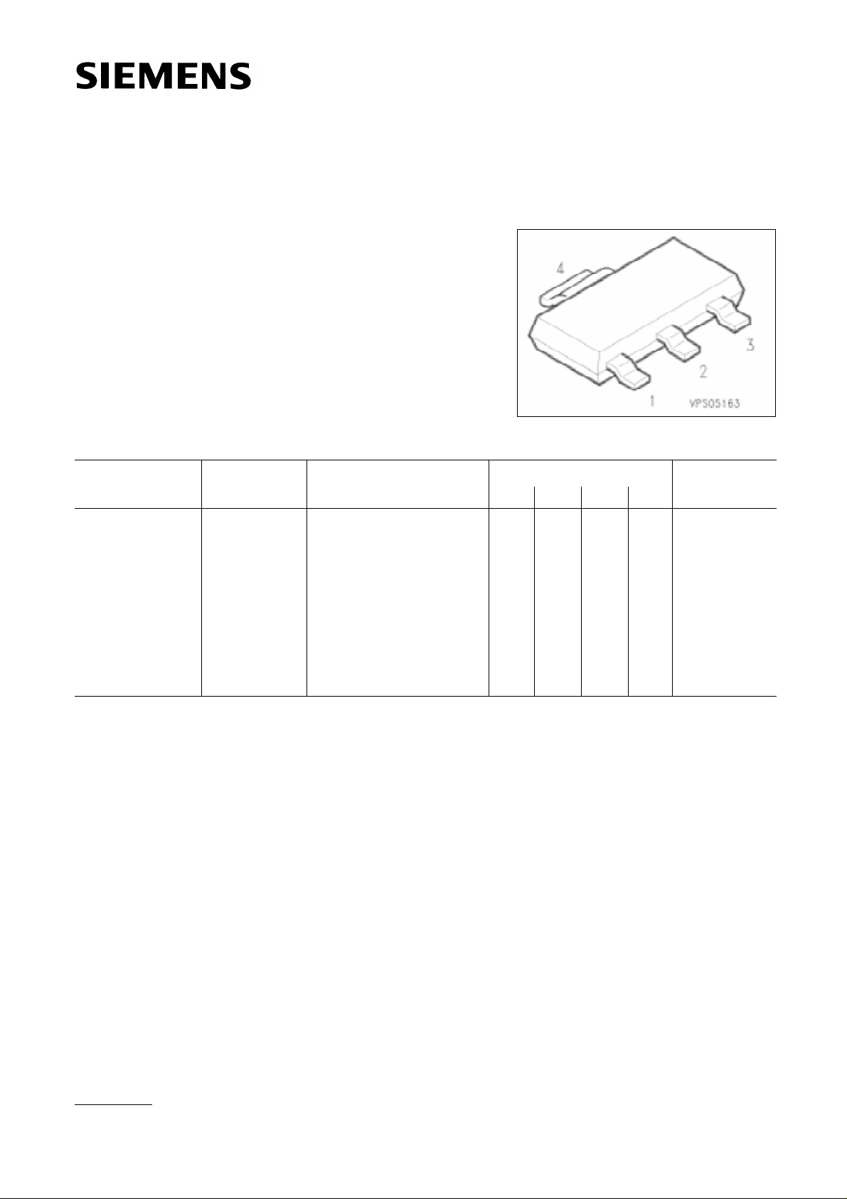
Pin Configuration
1 2 3
4
B C E C
Package
SOT-223
1)
1)
For detailed information see chapter Package Outlines.
Semiconductor Group 1
5.91
Page 2
Maximum Ratings
BCP 54
... BCP 56
Parameter Symbol
BCP 54
Collector-emitter voltage
BE ≤1kΩ
R
VCE0
VCER
45
45
Collector-base voltage VCB0 45
Emitter-base voltage V
EB0
Collector current IC A
Peak collector current I
Base current I
CM
B mA
Peak base current IBM
Total power dissipation, T
S =124 ˚C
1)
Junction temperature T
Storage temperature range T
Ptot W
j ˚C
stg – 65 … + 150
Values
BCP 55
60
60
60
5
1
1.5
100
200
1.5
150
BCP 56
80
100
100
Unit
V
Thermal Resistance
Junction - ambient
1)
Rth JA ≤ 72 K/W
Junction - soldering point Rth JS ≤ 17
1)
Package mounted on epoxy pcb 40 mm × 40 mm × 1.5 mm/6 cm2 Cu.
Semiconductor Group 2
Page 3

Electrical Characteristics
I
I
I
I
I
I
I
I
I
A = 25 ˚C, unless otherwise specified.
at T
DC characteristics
BCP 54
... BCP 56
UnitValuesParameter Symbol
min. typ. max.
(BR)CE0
V
C = 10 mA, IB = 0 BCP 54
BCP 55
BCP 56
Collector-base breakdown voltage
C = 100 µA, IB = 0 BCP 54
1)
(BR)CB0
V
BCP 55
BCP 56
V
Emitter-base breakdown voltage
E = 10 µA, IC = 0
Collector-base cutoff current
CB = 30 V, IE = 0
V
CB = 30 V, IE = 0, TA = 150 ˚C
V
EB = 5 V
V
(BR)EB0 5––
CB0
I
I
EB0 ––10
45
60
80
45
60
100
–
–
–
–
–
–
–
–
–
–
–
–
–
–
–
–
100
20
hFE
C = 5 mA, VCE = 2 V
C = 150 mA, VCE = 2 V
BCP 54/BCP 55/BCP 56
BCP 54/BCP 55/BCP 56-10
BCP 54/BCP 55/BCP 56-16
C = 500 mA, VCE = 2 V
25
40
63
100
25
–
–
100
160
–
–
250
160
250
–
VCollector-emitter breakdown voltage
nA
µA
µAEmitter-base cutoff current
–DC current gain
Collector-emitter saturation voltage
C = 500 mA, IB = 50 mA
Base-emitter voltage
C = 500 mA, VCE = 2 V
1)
1)
VCEsat – – 0.5
VBE ––1
V
AC characteristics
f
T – 100 –
C = 50 mA, VCE = 10 V, f = 100 MHz
MHzTransition frequency
1)
Pulse test conditions: t≤ 300 µs, D = 2 %.
Semiconductor Group 3
Page 4

BCP 54
... BCP 56
Total power dissipation Ptot = f (TA*; TS)
* Package mounted on epoxy
Transition frequency fT = f (IC)
CE = 10 V
V
DC current gain h
CE = 2 V
V
FE = f (IC)
Collector cutoff current I
CB = 30 V
V
CB0 = f (TA)
Semiconductor Group 4
Page 5

BCP 54
... BCP 56
Base-emitter saturation voltage
C = f (VBEsat)
I
FE = 10
h
Collector-emitter saturation voltage
C = f (VCEsat)
I
FE = 10
h
Permissible pulse load Ptot max/Ptot DC = f (tp)
Semiconductor Group 5
 Loading...