

Datasheet BC847CDXV6T1, BC847CDXV6T5, BC848CDXV6T1, BC848CDXV6T5 Datasheet (ON Semiconductor)
Page 1
BC847CDXV6T1,
BC847CDXV6T5
BC848CDXV6T1,
BC848CDXV6T5
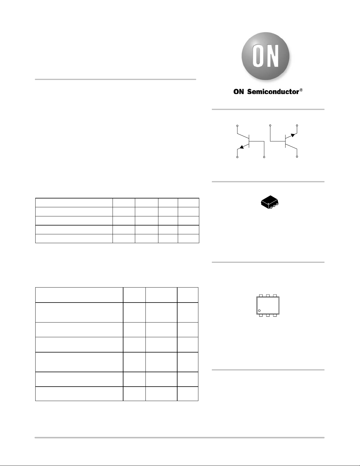
Dual General Purpose
Transistors
http://onsemi.com
NPN Duals
These transistors are designed for general purpose amplifier
applications. They are housed in the SOT−563 which is designed for
low power surface mount applications.
Features
• These are Pb−Free Devices
MAXIMUM RATINGS
Rating Symbol BC847 BC848 Unit
Collector − Emitter Voltage V
Collector − Base Voltage V
Emitter − Base Voltage V
Collector Current − Continuous I
Maximum ratings are those values beyond which device damage can occur.
Maximum ratings applied to the device are individual stress limit values (not
normal operating conditions) and are not valid simultaneously. If these limits are
exceeded, device functional operation is not implied, damage may occur and
reliability may be affected.
CEO
CBO
EBO
C
THERMAL CHARACTERISTICS
Characteristic
(One Junction Heated)
Total Device Dissipation, (Note 1)
TA = 25°C
Derate above 25°C
Thermal Resistance,
Junction-to-Ambient (Note 1)
Characteristic
(Both Junctions Heated)
Total Device Dissipation, (Note 1)
TA = 25°C
Derate above 25°C
Thermal Resistance,
Junction-to-Ambient (Note 1)
Junction and Storage
Temperature Range
1. FR−4 @ Minimum Pad
Symbol Max Unit
Symbol Max Unit
45 30 V
50 30 V
6.0 5.0 V
100 100 mAdc
P
D
R
q
JA
P
D
R
q
JA
TJ, T
− 55 to +150 °C
stg
357
2.9
350 °C/W
500
4.0
250 °C/W
mW
mW/°C
mW
mW/°C
(3)
Q
1
(4) (5) (6)
BC847CDXV6T1
6
1
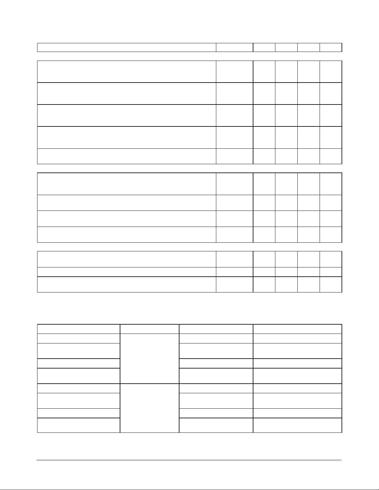
SOT−563
CASE 463A
PLASTIC
(1)(2)
Q
2
MARKING DIAGRAMS
1x M G
G
1
1x = Device Code
x = G or M
M = Date Code
G = Pb−Free Package
(Note: Microdot may be in either location)
ORDERING INFORMATION
See detailed ordering and shipping information in the package
dimensions section on page 2 of this data sheet.
© Semiconductor Components Industries, LLC, 2005
October, 2005 − Rev. 1
1 Publication Order Number:
BC847CDXV6T1/D
Page 2
BC847CDXV6T1, BC847CDXV6T5 BC848CDXV6T1, BC848CDXV6T5
ELECTRICAL CHARACTERISTICS (T
= 25°C unless otherwise noted)
A
Characteristic Symbol Min Typ Max Unit
OFF CHARACTERISTICS
Collector− Emitter Breakdown Voltage
(IC = 10 mA) BC847CDXV6T1
BC848CDXV6T1
Collector− Emitter Breakdown Voltage
(IC = 10 mA, VEB = 0) BC847CDXV6T1
BC848CDXV6T1
Collector− Base Breakdown Voltage
(IC = 10 mA) BC847CDXV6T1
BC848CDXV6T1
Emitter− Base Breakdown Voltage
(IE = 1.0 mA) BC847CDXV6T1
BC848CDXV6T1
Collector Cutoff Current (VCB = 30 V)
(VCB = 30 V, TA = 150°C)
ON CHARACTERISTICS
DC Current Gain
(IC = 10 mA, VCE = 5.0 V)
(IC = 2.0 mA, VCE = 5.0 V)
Collector− Emitter Saturation Voltage (IC = 10 mA, IB = 0.5 mA)
Collector− Emitter Saturation Voltage (IC = 100 mA, IB = 5.0 mA)
Base− Emitter Saturation Voltage (IC = 10 mA, IB = 0.5 mA)
Base− Emitter Saturation Voltage (IC = 100 mA, IB = 5.0 mA)
Base− Emitter Voltage (IC = 2.0 mA, VCE = 5.0 V)
Base− Emitter Voltage (IC = 10 mA, VCE = 5.0 V)
SMALL− SIGNAL CHARACTERISTICS
Current−Gain − Bandwidth Product
(IC = 10 mA, VCE = 5.0 Vdc, f = 100 MHz)
Output Capacitance (VCB = 10 V, f = 1.0 MHz) C
Noise Figure
(IC = 0.2 mA, VCE = 5.0 Vdc, RS = 2.0 kW,f = 1.0 kHz, BW = 200 Hz)
V
(BR)CEO
V
(BR)CES
V
(BR)CBO
V
(BR)EBO
I
CBO
h
V
CE(sat)
V
BE(sat)
V
BE(on)
f
obo
NF
FE
45
30
−
−
−
−
V
V
50
30
−
−
−
−
V
50
30
−
−
−
−
V
6.0
5.0
−
−
−
−
−
−
15
5.0
−
−
nA
mA
−
−
420
−
−
−
−
580
−
T
100 − − MHz
270
520
−
−
0.7
0.9
660
−
−
800
0.25
0.6
−
−
700
770
V
V
mV
− − 4.5 pF
dB
− − 10
ORDERING INFORMATION
Device Specific Marking Package Shipping
BC847CDXV6T1
BC847CDXV6T1G SOT−563
SOT−563 4000 Units / Tape & Reel
4000 Units / Tape & Reel
(Pb−Free)
BC847CDXV6T5 SOT−563 8000 Units / Tape & Reel
BC847CDXV6T5G SOT−563
1G
8000 Units / Tape & Reel
(Pb−Free)
BC848CDXV6T1
BC848CDXV6T1G SOT−563
SOT−563 4000 Units / Tape & Reel
4000 Units / Tape & Reel
(Pb−Free)
BC848CDXV6T5 SOT−563 8000 Units / Tape & Reel
BC848CDXV6T5G SOT−563
1L
8000 Units / Tape & Reel
(Pb−Free)
†For information on tape and reel specifications, including part orientation and tape sizes, please refer to our Tape and Reel Packaging
Specifications Brochure, BRD8011/D.
†
http://onsemi.com
2
Page 3

BC847CDXV6T1, BC847CDXV6T5 BC848CDXV6T1, BC848CDXV6T5
TYPICAL CHARACTERISTICS
2.0
1.5
1.0
0.8
0.6
0.4
, NORMALIZED DC CURRENT GAIN
0.3
FE
h
0.2
0.2 0.5 1.0 10 20
2.0 5.0
IC, COLLECTOR CURRENT (mAdc)
Figure 1. Normalized DC Current Gain
2.0
1.6
1.2
IC =
10 mA
0.8
IC = 50 mA IC = 100 mA
IC =
20 mA
VCE = 10 V
TA = 25°C
50
IC = 200 mA
100
200
V, VOLTAGE (VOLTS)
1.0
TA = 25°C
0.9
0.8
0.7
0.6
0.5
0.4
0.3
0.2
0.1
0
0.2 0.5 1.0 10 20
V
@ IC/IB = 10
BE(sat)
V
@ VCE = 10 V
BE(on)
V
@ IC/IB = 10
CE(sat)
2.0
IC, COLLECTOR CURRENT (mAdc)
Figure 2. “Saturation” and “On” Voltages
1.0
−55°C to +125°CTA = 25°C
1.2
1.6
2.0
2.4
50
307.05.03.00.70.30.1
10070
0.4
, COLLECTOR−EMITTER VOLTAGE (V)
CE
V
0.02 1.0
0.1
IB, BASE CURRENT (mA)
Figure 3. Collector Saturation Region
10
7.0
5.0
3.0
2.0
C, CAPACITANCE (pF)
1.0
0.4 0.6 1.0 10 20
0.8 4.0 8.0
C
ib
C
ob
2.0 6.0
VR, REVERSE VOLTAGE (VOLTS)
Figure 5. Capacitances
TA = 25°C
10020
2.8
, TEMPERATURE COEFFICIENT (mV/ C)°θ
VB
0.2 1.0
IC, COLLECTOR CURRENT (mA)
10 100
Figure 4. Base−Emitter Temperature Coefficient
400
300
200
100
80
60
40
30
20
T
f, CURRENT−GAIN − BANDWIDTH PRODUCT (MHz)
40
0.7 1.0 10 202.0
IC, COLLECTOR CURRENT (mAdc)
VCE = 10 V
TA = 25°C
307.05.03.00.5
50
Figure 6. Current−Gain − Bandwidth Product
http://onsemi.com
3
Page 4

BC847CDXV6T1, BC847CDXV6T5 BC848CDXV6T1, BC848CDXV6T5
PACKAGE DIMENSIONS
SOT−563, 6 LEAD
CASE 463A−01
ISSUE F
D
−X−
45L6
12 3
e
E
−Y−
b 6 5 PL
0.08 (0.003) X
M
Y
A
H
E
C
SOLDERING FOOTPRINT*
0.3
0.0118
1.0
1.35
0.0531
0.0394
NOTES:
1. DIMENSIONING AND TOLERANCING PER ANSI
Y14.5M, 1982.
2. CONTROLLING DIMENSION: MILLIMETERS
3. MAXIMUM LEAD THICKNESS INCLUDES LEAD
FINISH THICKNESS. MINIMUM LEAD THICKNESS
IS THE MINIMUM THICKNESS OF BASE MATERIAL.
MILLIMETERS
DIM MIN NOM MAX
A 0.50 0.55 0.60
b 0.17 0.22 0.27
C
0.08 0.12 0.18 0.003 0.005 0.007
D 1.50 1.60 1.70
E 1.10 1.20 1.30
e 0.5 BSC
L 0.10 0.20 0.30
H
1.50 1.60 1.70
E
STYLE 1:
PIN 1. EMITTER 1
2. BASE 1
3. COLLECTOR 2
4. EMITTER 2
5. BASE 2
6. COLLECTOR 1
INCHES
MIN NOM MAX
0.020 0.021 0.023
0.007 0.009 0.011
0.059 0.062 0.066
0.043 0.047 0.051
0.02 BSC
0.004 0.008 0.012
0.059 0.062 0.066
0.45
0.0177
0.5
0.5
0.0197
0.0197
SCALE 20:1
ǒ
inches
mm
Ǔ
*For additional information on our Pb−Free strategy and soldering
details, please download the ON Semiconductor Soldering and
Mounting Techniques Reference Manual, SOLDERRM/D.
ON Semiconductor and are registered trademarks of Semiconductor Components Industries, LLC (SCILLC). SCILLC reserves the right to make changes without further notice
to any products herein. SCILLC makes no warranty, representation or guarantee regarding the suitability of its products for any particular purpose, nor does SCILLC assume any liability
arising out of the application or use of any product or circuit, and specifically disclaims any and all liability, including without limitation special, consequential or incidental damages.
“Typical” parameters which may be provided in SCILLC data sheets and/or specifications can and do vary in different applications and actual performance may vary over time. All
operating parameters, including “Typicals” must be validated for each customer application by customer’s technical experts. SCILLC does not convey any license under its patent rights
nor the rights of others. SCILLC products are not designed, intended, or authorized for use as components in systems intended for surgical implant into the body, or other applications
intended to support or sustain life, or for any other application in which the failure of the SCILLC product could create a situation where personal injury or death may occur. Should
Buyer purchase or use SCILLC products for any such unintended or unauthorized application, Buyer shall indemnify and hold SCILLC and its officers, employees, subsidiaries, affiliates,
and distributors harmless against all claims, costs, damages, and expenses, and reasonable attorney fees arising out of, directly or indirectly, any claim of personal injury or death
associated with such unintended or unauthorized use, even if such claim alleges that SCILLC was negligent regarding the design or manufacture of the part. SCILLC is an Equal
Opportunity/Affirmative Action Employer. This literature is subject to all applicable copyright laws and is not for resale in any manner.
PUBLICATION ORDERING INFORMATION
LITERATURE FULFILLMENT:
Literature Distribution Center for ON Semiconductor
P.O. Box 61312, Phoenix, Arizona 85082−1312 USA
Phone: 480−829−7710 or 800−344−3860 Toll Free USA/Canada
Fax: 480−829−7709 or 800−344−3867 Toll Free USA/Canada
Email: orderlit@onsemi.com
N. American Technical Support: 800−282−9855 Toll Free
USA/Canada
Japan: ON Semiconductor, Japan Customer Focus Center
2−9−1 Kamimeguro, Meguro−ku, Tokyo, Japan 153−0051
Phone: 81−3−5773−3850
http://onsemi.com
ON Semiconductor Website: http://onsemi.com
Order Literature: http://www.onsemi.com/litorder
For additional information, please contact your
local Sales Representative.
BC847CDXV6T1/D
4
 Loading...