

Page 1
LESHAN RADIO COMPANY, LTD.
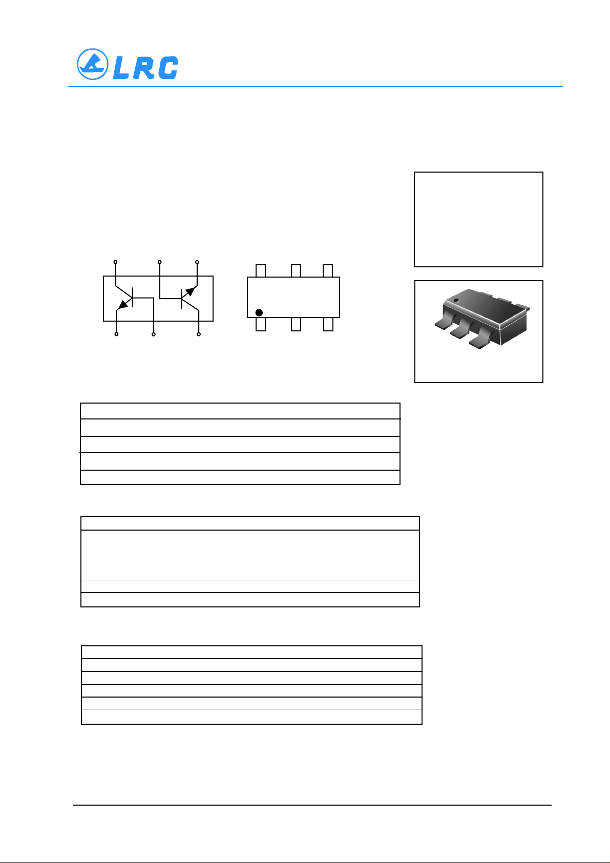
Dual General Purpose Transistors
NPN Duals
These transistors are designed for general purpose amplifier
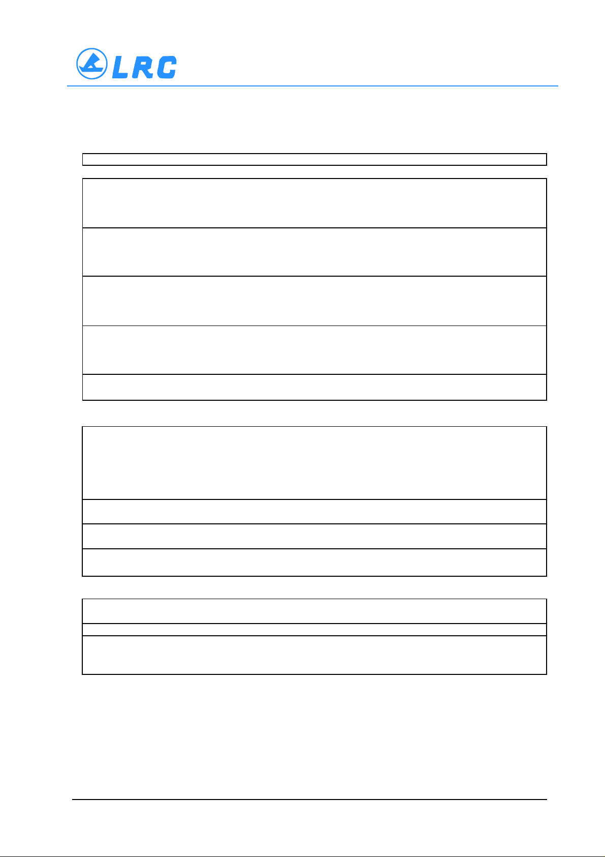
applications. They are housed in the SOT–363/SC–88 which is
designed for low power surface mount applications.
6
Q
2
1
MAXIMUM RATINGS
Rating Symbol BC846 BC847 BC848 Unit
Collector–Emitter Voltage V
Collector–Base Voltage V
Emitter–Base Voltage V
Collector Current -Continuous I
5
2
4
Q
1
3
CEO
CBO
EBO
C
See Table
65 45 30 V
80 50 30 V
6.0 6.0 5.0 V
100 100 100 mAdc
BC846BDW1T1
BC847BDW1T1
BC847CDW1T1
BC848BDW1T1
BC848CDW1T1
6
5
1
2
3
SOT-363 /SC-88
CASE 419B STYLE1
4
THERMAL CHARACTERISTICS
Characteristic Symbol Max Unit
T otal Device Dissipation P
Per Device 250 mW
FR– 5 Board, (1) TA = 25°C
Derate above 25°C 3.0 mW/°C
Thermal Resistance, Junction to Ambient R
Junction and Storage Temperature T J , T
1. FR–5 = 1.0 x 0.75 x 0.062 in.
D
θJA
stg
380 mW
328 °C/W
–55 to +150 °C
ORDERING INFORMATION
Device Package Shipping
BC846BDW1T1 SOT–363 3000 Units/ Reel
BC847BDW1T1 SOT–363 3000 Units/ Reel
BC847CDW1T1 SOT–363 3000 U nits/R eel
BC848BDW1T1 SOT–363 3000 Units/ Reel
BC848CDW1T1 SOT–363 3000 U nits/R eel
BC846b–1/5
Page 2
LESHAN RADIO COMPANY, LTD.
BC846BDW1T1, BC847BDW1T1, BC847CDW1T1, BC848BDW1T1, BC848CDW1T1
ELECTRICAL CHARACTERISTICS (T
= 25°C unless otherwise noted)
A
Characteristic Symbol Min Typ Max Unit
OFF CHARACTERISTICS
Collector–Emitter Breakdown Voltage V
(I C = 10 mA) BC846 Series 65 — —
BC847 Series 45 — —
BC848 Series 30 — —
Collector–Emitter Breakdown Voltage V
(I C = 10 µA, V
= 0) BC846 Series 80 — —
EB
BC847 Series 50 — —
BC848 Series 30 — —
Collector–Base Breakdown Voltage V
(I C = 10 µA) BC846 Series 80 — —
BC847 Series 50 — —
BC848 Series 30 — —
Emitter–Base Breakdown Voltage V
(I E = 1.0 µA) BC846 Series 6.0 — —
BC847 Series 6.0 — —
BC848 Series 5.0 — —
Collector Cutoff Current (V
= 30 V) I
CB
(V
= 30 V, T A = 150°C) — — 5.0 µA
CB
(BR)CEO
(BR)CES
(BR)CBO
(BR)EBO
CBO
——15nA
ON CHARACTERISTICS
DC Current Gain h
(I C = 10 µA, V
= 5.0 V) BC846B, BC847B, BC848B — 150 —
CE
BC847C, BC848C — 270 —
FE
V
V
V
V
—
(I C = 2.0 mA, V
= 5.0 V) BC846B, BC847B, BC848B 200 290 450
CE
BC847C, BC848C 420 520 800
Collector–Emitter Saturation Voltage (I C = 10 mA, I B = 0.5 mA) V
CE(sat)
— — 0.25 V
Collector–Emitter Saturation Voltage ( I C = 100 mA, I B = 5.0 mA) — — 0.6
Base–Emitter Saturation Voltage (I C = 10 mA, I B = 0.5 mA) V
BE(sat)
— 0.7 — V
Base–Emitter Saturation Voltage (I C = 100 mA, I B = 5.0 mA) — 0.9 —
Base–Emitter Voltage (I C = 2.0 mA, V
Base–Emitter Voltage (I C = 10 mA, V
= 5.0 V) V
CE
= 5.0 V) — — 770
CE
BE(on)
580 660 700 mV
SMALL–SIGNAL CHARACTERISTICS
Current–Gain — Bandwidth Product f
(I C = 10 mA, V
Output Capacitance (V
= 5.0 Vdc, f = 100 MHz)
CE
= 10 V, f = 1.0 MHz) C
CB
T
obo
Noise Figure (I C = 0.2 mA, NF dB
V
= 5.0 V dc, R S = 2.0 kΩ, BC846B, BC847B, BC848B — — 10
CE
f = 1.0 kHz, BW = 200 Hz) BC847C, BC848C — — 4.0
100 — — MHz
— — 4.5 pF
BC846b–2/5
Page 3

LESHAN RADIO COMPANY, LTD.
BC846BDW1T1, BC847BDW1T1, BC847CDW1T1, BC848BDW1T1, BC848CDW1T1
TYPICAL CHARACTERISTICS
2.0
1.5
1.0
0.8
0.6
0.4
0.3
h FE , NORMALIZED DC CURRENT GAIN
0.2
0.2 0.5 1.0 2.0 5.0 10 20 50 100 200
I C , COLLECTOR CURRENT (mAdc)
Figure 1. Normalized DC Current Gain
2.0
1.6
1.2
0.8
1.0
0.9
0.8
0.7
0.6
0.5
0.4
0.3
0.2
V,VOLTAGE (VOLTS)
0.1
0
0.1 0.2 0.3 0.50.71.0 2.0 3.0 5.07.0 10 20 30 50 70100
I C , COLLECTOR CURRENT (mAdc)
Figure 2. “Saturation” and “On” Voltages
1.0
1.2
1.6
2.0
2.4
0.4
, COLLECTOR-EMITTER VOL TAGE(V)
CE
0
V
0.02 0.1 1.0 10 20
I B , BASE CURRENT (mA)
Figure 3. Collector Saturation Region
2.8
, TEMPERA TURE COEFFICIENT (mV/ ° C)
vb
θ
0.2 1.0 10 100
I C , COLLECTOR CURRENT (mA)
Figure 4. Base–Emitter Temperature Coefficient
BC846b–3/5
Page 4

LESHAN RADIO COMPANY, LTD.
BC846BDW1T1, BC847BDW1T1, BC847CDW1T1, BC848BDW1T1, BC848CDW1T1
TYPICAL CHARACTERISTICS
10
7.0
5.0
3.0
2.0
C,CAPACITANCE(pF)
1.0
0.4 0.6 0.81.0 2.0 4.0 6.0 8.0 10 20 40
V R , REVERSE VOLTAGE (VOLTS)
Figure 5. Capacitances
2.0
1.0
0.5
0.2
, DC CURRENT GAIN (NORMALIZED)
FE
h
0.1 0.2 1.0 10 100
I C , COLLECTOR CURRENT (mA)
Figure 7. DC Current Gain
400
300
200
100
80
60
40
30
20
0.5 0.7 1.0 2.0 3.0 5.0 7.0 10 20 30 50
, CURREN-GAIN-BANDWIDTH PRODUCT (MHz)
f
T
I C , COLLECTOR CURRENT (mAdc)
Figure 6. Current–Gain – Bandwidth Product
1.0
0.8
0.6
0.4
V, VOLTAGE (VOLTS)
0.2
0
0.2 0.5 1.0 2.0 5.0 10 20 50 100 200
I C , COLLECTOR CURRENT (mA)
Figure 8. “On” Voltage
2.0
1.6
1.2
0.8
0.4
, COLLECTOR-EMITTER VOLTAGE(VOL TS)
CE
0
V
0.02 0.05 0.1 0.2 0.5 1.0 2.0 5.0 10 20
I B , BASE CURRENT (mA)
Figure 9. Collector Saturation Region
-1.0
-1.4
-1.8
-2.2
-2.6
, TEMPERATURE COEFFICIENT (mV/ ° C)
-3.0
VB
θ
0.2 0.5 1.0 2.0 5.0 10 20 50 100 200
I C , COLLECTOR CURRENT (mA)
Figure 10. Base–Emitter Temperature Coefficient
BC846b–4/5
Page 5

LESHAN RADIO COMPANY, LTD.
BC846BDW1T1, BC847BDW1T1, BC847CDW1T1, BC848BDW1T1, BC848CDW1T1
1.0
D=0.5
0.2
0.1
0.1
0.05
0.02
0.01
0.01
r(t), TRANSIENT THERMAL
RESISTANCE (NORMALIZED)
0.001
SINGLE PULSE
0 1.0 10 100 1.0K 10K 100K 1.0M
P
(pk)
t
1
t
2
DUTY CYCLE, D = t 1 /t
2
t, TIME (ms)
Figure 11. Thermal Response
-200
The safe operating area curves indicate I C –V
-100
thetransistor that must be observed for reliable operation.
Collector load lines for specific circuits must fall below the
-50
limits indicated by the applicable curve.
The data of Figure 12 is based upon T
T A is variable depending upon conditions. Pulse curves are
-10
valid for duty cycles to 10% provided T
(pk) may be calculated from the data in Figure 12. At high
-5.0
, COLLECTOR CURRENT (mA)
C
I
-2.0
-1.0 -5.0 -10 -30 -45 -65 -100
V
, COLLECTOR–EMITTER VOLTAGE (V)
CE
case or ambient temperatures, thermal limitations will reduce
the power that can be handled to values less than the limitations imposed by the secondary breakdown.
Figure 12. Active Region Safe Operating Area
Z
(t) = r(t) R
θJA
R
θJA
D CURVES APPLY FOR POWER
PULSE TRAIN SHOWN
READ TIME AT t
T
J(pk)
θJA
= 328°C/W MAX
– T C = P
1
R
(pk)
= 150°C; T C or
J(pk)
< 150°C. T
J(pk)
θJC
CE
(t)
limits of
J
BC846b–5/5
 Loading...