

Page 1
3
1997 Fairchild Semiconductor Corporation
BC846A / BC846B / BC847A / BC847B / BC847C
NPN General Purpose Amplifier
This device is designed for low noise, high gain, general purpose
amplifier applications at collector currents from 1.0 µA to 50 mA.
Sourced from Process 07.
Absolute Maximum Ratings* TA = 25°C unless otherwise noted
*These ratings are limiting values above which the serviceability of any semiconductor device may be impaired.
NOTES:
1) These ratings are based on a maximum junction temperature of 150 degrees C.
2) These are steady state limits. The factory should be consulted on applications involving pulsed or low duty cycle operations.
Thermal Characteristics TA = 25°C unless otherwise noted
Symbol Parameter Value Units
V
CEO
Collector-Emitter Voltage
BC846 series
BC847 series
65
45
V
V
V
CES
Collector-Base Voltage
BC846 series
BC847 series
80
50
V
V
V
EBO
Emitter-Base Voltage 6.0 V
I
C
Collector Current - Continuous 100 mA
TJ, T
stg
Operating and Stora ge Junction Temperature Range -55 to +150
°
C
Symbol Characteristic Max Units
*BC846 / BC847
P
D
Total Devi ce Dissi pation
Derate above 25°C
325
2.8
mW
mW/°C
R
θ
JA
Thermal Resistance , Junctio n to Ambient 357
°
C/W
BC847A
BC847B
BC847C
SOT-23
Mark: 1E. / 1F. / 1G.
C
B
E
C
B
E
BC846A
BC846B
SOT-23
Mark: 1A. / 1B.
*Device mounted on FR-4 PCB 40 mm X 40 mm X 1.5 mm.
Page 2
T ypical Characteristics
Electrical Characteristics
TA = 25°C unless otherwise noted
OFF CHARACTERISTICS
Symbol Parameter Test Conditions Min Max Units
V
(BR)CEO
Collector-Emitter Breakdown
Voltage
I
C
= 10 mA, IB = 0
846A / B
847A / B
65
45
V
V
(BR)CES
Collector-Base Breakdown Voltage
I
C
= 10 µA, IE = 0
846A / B
847A / B
80
50
V
V
(BR)EBO
Emitter-Base Breakdown Voltage
I
E
= 10 µA, IC = 0
6.0 V
I
CBO
Collector-Cutoff Current VCB = 30 V
V
CB
= 30 V, TA = 150°C
15
5.0
nA
µA
ON CHARACTERISTICS
h
FE
DC Current Gain IC = 2.0 mA, VCE = 5.0 V
846A / 847A
846B / 847B
847C
110
200
420
220
450
800
V
CE(
sat
)
Collector-Emitter Saturation Voltage IC = 10 mA, IB = 0.5 mA
I
C
= 100 mA, IB = 5.0 mA
0.25
0.6
V
V
V
BE(on)
Base-Emitter On Voltage IC = 2.0 mA, VCE = 5.0 V
I
C
= 10 mA, VCE = 5.0 V
0.58 0.70
0.77
V
V
SMALL SIGNAL CHARACTERISTICS
f
T
Current Gain - Bandwidth Product IC = 10 mA, VCE = 5.0,
f = 100 MHz
100 MHz
C
obo
Output Capacitance VCB = 10 V, f = 1.0 MHz 4.5 pF
NF Noise Figure IC = 0.2 mA, VCE = 5.0,
R
S
= 2.0 kΩ, f = 1.0 kHz,
BW = 200 Hz
10 dB
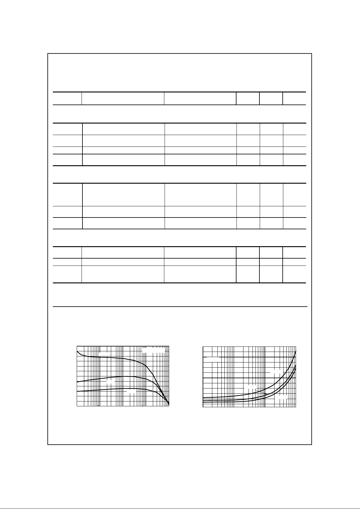
Collector-Emitter Sat urati on
Voltage vs Collector Current
0.1 1 10 100
0.05
0.1
0.15
0.2
0.25
0.3
I - COLLECTOR CURRENT (mA)
V - COLLECTOR-EMITTER VOLTAGE (V)
C
CESAT
25 °C
- 40 °C
125 °C
β
= 10
Typical Pulsed Current Gain
vs Collector Current
0.01 0.03 0.1 0.3 1 3 10 30 100
0
200
400
600
800
1000
1200
I - COLLECTOR CURRENT (mA)
h - TYPICAL PULSED CUR REN T GAIN
C
FE
125 °C
25 °C
- 40 °C
V = 5.0 V
CE
BC846A / BC846B / BC847A / BC847B / BC847C
NPN General Purpose Amplifier
(continued)
Page 3
3
BC846A / BC846B / BC847A / BC847B / BC847C
T ypical Characteristics
NPN General Purpose Amplifier
(continued)
Input and Output Capacitance
vs Reverse Bias Voltage
048121620
0
1
2
3
4
5
REVERSE BIAS VOLTAGE (V)
CAP ACITANCE (pF)
f = 1.0 MHz
C
ob
C
te
Wideband Noise Frequency
vs Source Resistance
1,000 2,000 5,000 10,000 20,000 50,000 100,000
0
1
2
3
4
5
R - SOURCE RESISTANCE ( )
NF - NOI S E FI GU RE ( d B)
V = 5.0 V
BANDWI DT H = 1 5.7 kH z
CE
I = 10 µA
C
I = 100 µA
C
S
Ω
I = 30 µA
C
Base-Emitter Saturation
Voltage vs Collector Curr en t
0.1 1 10 100
0.2
0.4
0.6
0.8
1
I - COLLECT OR CURRENT (mA)
V - COLLECTOR-EMITTER VOLTAGE (V)
C
BESAT
β
= 10
25 °C
- 40 °C
125 °C
Base-Emitter ON Voltage vs
Collector Current
0.1 1 10 40
0.2
0.4
0.6
0.8
1
I - COLLECTOR CURRENT (mA)
V - BASE-EMITTER ON VOLTAGE (V)
C
BEON
V = 5.0 V
CE
25 °C
- 40 °C
125 °C
Collect or-Cutoff Current
vs Amb ient Temperature
25 50 75 100 125 150
0.1
1
10
T - A M BI E NT T EMP ER AT UR E ( C)
I - COLLECTOR CURRENT (nA)
A
CBO
V = 45V
°
CB
Normalized Collector-Cutoff Current
vs Ambient Temp er ature
25 50 75 100 125 150
1
10
100
1000
T - AMBIENT TEMPERATURE ( C)
CHARACTERIS TIC S RELATIVE TO VALUE AT T = 25 C
A
A
°
°
Page 4
Contours of Constant Gain
Bandwidth Pr oduct ( f )
0.1 1 10 100
1
2
3
5
7
10
I - COLLECTOR CURRENT (mA)
V - COLLECTOR VOLTAGE (V)
C
175 MHz
T
CE
150 MHz
125 MHz
75 MHz
100 MHz
Typical Characteristics (continued)
Contours of Consta n t
Narrow Band Noise Figure
1 10 100 1,000
100
200
500
1,000
2,000
5,000
10,000
I - COLLECTOR CURRENT ( A)
R - SOURCE RESISTANCE ( )
µ
C
Ω
S
V = 5.0 V
f = 1.0 kHz
BANDWIDTH
= 200 Hz
CE
6.0 dB
3.0 dB
4.0 dB
8.0 dB
2.0 dB
Contours of Constant
Narrow Band Noise Figure
1 10 100 1,000
100
200
500
1,000
2,000
5,000
10,000
I - COLLECTOR CURRENT ( A)
R - SOURC E RESISTANCE ( )
µ
C
Ω
S
V = 5. 0 V
f = 100 Hz
BANDWIDTH
= 20 Hz
CE
3.0 dB
4.0 dB
8.0 dB
10 dB
12 dB
14 dB
6.0 dB
Contours of Constant
Nar r ow Band No is e Figure
1 10 100 1000
100
200
500
1000
2000
5000
10000
I - COLL E CTOR CURR ENT ( A)
R - SOURCE RESISTANCE ( )
6.0 dB
3.0 dB
4.0 dB
8.0 dB
2.0 dB
1.0 dB
C
V = 5.0V
f = 10kHz
BANDWIDTH
= 2.0kHz
CE
Ω
S
µ
Contours of Constant
Nar row Band No ise Fi gure
0.01 0.1 1 10
100
200
500
1000
2000
5000
10000
I - COLLEC TO R CU RRENT ( A)
R - SOURCE RESISTANCE ( )
7.0 dB
3.0 dB
4.0 dB
8.0 dB
2.0 dB
5.0
dB
C
V =
5.0V
CE
Ω
S
µ
f = 1.0 MHz
BANDW IDTH
= 200kHz
6.0
dB
Noise Figure vs Frequency
0.0001 0.001 0.01 0.1 1 10 100
0
2
4
6
8
10
f - FREQUENCY (MHz)
NF - NOI S E FI GU RE ( d B)
V = 5.0V
CE
I = 200 µA,
R = 10 k
Ω
C
S
I = 1.0 mA,
R = 500
Ω
C
S
I = 100 µA,
R = 10 k
Ω
C
S
I = 1.0 mA,
R = 5.0 k
Ω
C
S
BC846A / BC846B / BC847A / BC847B / BC847C
NPN General Purpose Amplifier
(continued)
Page 5

3
BC846A / BC846B / BC847A / BC847B / BC847C
NPN General Purpose Amplifier
(continued)
Typical Common Emitter Characteristics (f = 1.0 kHz)
Typical Common Emitter Characteristics
0.1 0.2 0.5 1 2 5 10 20 50 100
0.01
0.1
1
10
100
I - COLLECTOR CURRENT (mA)
CHARACTERISTICS RELAT IVE TO VAL U E( I =1mA)
C
C
f = 1.0kHz
h
oe
h
oe
h and h
ie
h
fe
h
re
h
ie
h
fe
re
Typic al Common Emitter Characteristics
-100 -50 0 50 100 150
0.5
0.6
0.7
0.8
0.9
1
1.1
1.2
1.3
1.4
1.5
T - JU NC T IO N TEMP ERATURE ( C)
CHARACTERISTICS RE LATIVE TO VALUE(T =25 C)
J
A
°
h
oe
h
re
h
ie
h
fe
h
oe
h
re
h
ie
h
fe
V = 5.0V
f = 1.0kHz
I = 1 .0mA
CE
C
°
Typical C o mmo n Emi tter Char a cteri stics
0 5 10 15 20 25
0.8
0.9
1
1.1
1.2
1.3
1.4
V - COLL EC TOR V OLTAGE (V )
CH AR ACTERISTICS RELATIVE T O VALUE(V =5V)
CE
CE
I = 1 .0mA
f = 1. 0k Hz
T = 25 C
C
A
°
h
oe
h
oe
h
re
h
ie
h
fe
h
re
h
ie
h
fe
Page 6

SOT-23 Packaging
Configuration: F igur e 1.0
Components
Leader Tape
500mm minimum or
125 empty pockets
Trailer Tape
300mm minimum or
75 empty pocket s
SOT-23 Tape Leader and Trailer
Configuration: Figure 2.0
Cover Tape
Carrier Tape
Note/Comments
Packaging Option
SOT-23 Packaging Information
Stan dard
(no flow code)
D87Z
Packaging type
Reel Size
TNR
7" Dia
TNR
13"
Qty per Reel/Tube/Bag
3,000 10,000
Box Dimensi on (mm)
187x107x183 343x343x64
Max qty per B ox
24,000 30,000
Weight per unit (gm)
0.0082 0.0082
Weight per Reel (kg)
0.1175 0.4006
Human readable
Label
Human Readable Label
Human Readable Label sampl e
343mm x 342mm x 64mm
Intermediate box for L87Z Option
187mm x 107mm x 183mm
Intermediate Box for Standard Option
SOT-23 Unit Orientation
3P 3P 3P 3P
Human Readable
Label
Customiz ed Label
Embossed
Carrier Tape
Antistatic Cover Tape
Packaging Description:
SOT-23
made from a dissipative (carbon filled) polycarbonate
resin. The cover tape is a multilayer film (Heat Activated
Adhesive in nature) primarily composed of polyester film,
adhesive layer, sealant, and anti-static sprayed agent.
These reeled parts in standard option are shipped with
3,000 units per 7" or 177cm diameter reel. The reels are
dark blue in color and is made of polystyrene plastic (antistatic coated). Other option comes in 10,000 units per 13"
or 330cm diameter r eel. This and some other options are
described in the Packaging Information table.
These full reels are individually labeled and placed inside
a st andard intermediate made of recyclable corrugated
brown paper with a Fairchild l ogo printing. One pizza box
contains eight reels maximum. And these intermediate
boxes are placed inside a labeled shipping box which
comes in diff erent sizes depending on the number of parts
shipped.
parts are shipped in tape. The carrier tape is
SOT-23 Tape and Reel Data
September 1999, Rev. C
©2000 Fairchild Semiconductor International
Page 7

Dimensions are in millimeter
Pkg type
A0 B0 W D0 D1 E1 E2 F P1 P0 K0 T Wc Tc
SOT-23
(8mm)
3.15
+/-0.10
2.77
+/-0.10
8.0
+/-0.3
1.55
+/-0.05
1.125
+/-0.125
1.75
+/-0.10
6.25
min
3.50
+/-0.05
4.0
+/-0.1
4.0
+/-0.1
1.30
+/-0.10
0.228
+/-0.013
5.2
+/-0.3
0.06
+/-0.02
Dimensions are in inches and millimeters
Tape Size
Reel
Option
Dim A Dim B Dim C Dim D Dim N Dim W1 Dim W2 Dim W3 (LSL-USL)
8mm 7" Dia
7.00
177.8
0.059
1.5
512 +0.020/-0.008
13 +0.5/-0.2
0.795
20.2
2.165550.331 +0.059/-0.000
8.4 +1.5/0
0.567
14.4
0.311 – 0.429
7.9 – 10.9
8mm 13" Dia
13.00
330
0.059
1.5
512 +0.020/-0.008
13 +0.5/-0.2
0.795
20.2
4.00
100
0.331 +0.059/-0.000
8.4 +1.5/0
0.567
14.4
0.311 – 0.429
7.9 – 10.9
See detail AA
Dim A
max
13" Diameter Option
7"
Diameter Option
Dim A
Max
See detail AA
W3
W2 max Measured at Hub
W1 Measured at Hub
Dim N
Dim D
min
Dim C
B Min
DETAIL AA
Notes: A0, B0, and K0 dimensions are determined with respect to the EIA/Jedec RS-481
rotational and lateral movement requirements (see sketches A, B, and C).
20 deg maximum component rotation
0.5mm
maximum
0.5mm
maximum
Sketch C (Top View)
Component lateral movement
Typical
component
cavity
center line
20 deg maximum
Typical
component
center line
B0
A0
Sketch B (Top View)
Component Rotation
Sketch A (Side or Front Sectional View)
Component Rotation
User Direction of Feed
SOT-23 Embossed Carrier Tape
Configuration: Figure 3.0
SOT-23 Reel Configuration: Figure 4.0
P1
A0
D1
F
W
E1
E2
Tc
Wc
K0
T
B0
D0P0 P2
SOT-23 Tape and Reel Data, continued
September 1999, Rev. C
Page 8

SOT-23 (FS PKG Code 49)
SOT-23 Package Dimensions
September 1998, Rev . A1
1:1
Scale 1:1 on letter size paper
Dimensions shown below are in:
inches [millimeters]
Part Weight per unit (gram): 0.0082
©2000 Fairchild Semiconductor International
Page 9

SOT-23 Packaging
Configuration: F igur e 1.0
Components
Leader Tape
500mm minimum or
125 empty pockets
Trailer Tape
300mm minimum or
75 empty pocket s
SOT-23 Tape Leader and Trailer
Configuration: Figure 2.0
Cover Tape
Carrier Tape
Note/Comments
Packaging Option
SOT-23 Packaging Information
Stan dard
(no flow code)
D87Z
Packaging type
Reel Size
TNR
7" Dia
TNR
13"
Qty per Reel/Tube/Bag
3,000 10,000
Box Dimensi on (mm)
187x107x183 343x343x64
Max qty per B ox
24,000 30,000
Weight per unit (gm)
0.0082 0.0082
Weight per Reel (kg)
0.1175 0.4006
Human readable
Label
Human Readable Label
Human Readable Label sampl e
343mm x 342mm x 64mm
Intermediate box for L87Z Option
187mm x 107mm x 183mm
Intermediate Box for Standard Option
SOT-23 Unit Orientation
3P 3P 3P 3P
Human Readable
Label
Customiz ed Label
Embossed
Carrier Tape
Antistatic Cover Tape
Packaging Description:
SOT-23
made from a dissipative (carbon filled) polycarbonate
resin. The cover tape is a multilayer film (Heat Activated
Adhesive in nature) primarily composed of polyester film,
adhesive layer, sealant, and anti-static sprayed agent.
These reeled parts in standard option are shipped with
3,000 units per 7" or 177cm diameter reel. The reels are
dark blue in color and is made of polystyrene plastic (antistatic coated). Other option comes in 10,000 units per 13"
or 330cm diameter r eel. This and some other options are
described in the Packaging Information table.
These full reels are individually labeled and placed inside
a st andard intermediate made of recyclable corrugated
brown paper with a Fairchild l ogo printing. One pizza box
contains eight reels maximum. And these intermediate
boxes are placed inside a labeled shipping box which
comes in diff erent sizes depending on the number of parts
shipped.
parts are shipped in tape. The carrier tape is
SOT-23 Tape and Reel Data
September 1999, Rev. C
©2000 Fairchild Semiconductor International
Page 10

Dimensions are in millimeter
Pkg type
A0 B0 W D0 D1 E1 E2 F P1 P0 K0 T Wc Tc
SOT-23
(8mm)
3.15
+/-0.10
2.77
+/-0.10
8.0
+/-0.3
1.55
+/-0.05
1.125
+/-0.125
1.75
+/-0.10
6.25
min
3.50
+/-0.05
4.0
+/-0.1
4.0
+/-0.1
1.30
+/-0.10
0.228
+/-0.013
5.2
+/-0.3
0.06
+/-0.02
Dimensions are in inches and millimeters
Tape Size
Reel
Option
Dim A Dim B Dim C Dim D Dim N Dim W1 Dim W2 Dim W3 (LSL-USL)
8mm 7" Dia
7.00
177.8
0.059
1.5
512 +0.020/-0.008
13 +0.5/-0.2
0.795
20.2
2.165550.331 +0.059/-0.000
8.4 +1.5/0
0.567
14.4
0.311 – 0.429
7.9 – 10.9
8mm 13" Dia
13.00
330
0.059
1.5
512 +0.020/-0.008
13 +0.5/-0.2
0.795
20.2
4.00
100
0.331 +0.059/-0.000
8.4 +1.5/0
0.567
14.4
0.311 – 0.429
7.9 – 10.9
See detail AA
Dim A
max
13" Diameter Option
7"
Diameter Option
Dim A
Max
See detail AA
W3
W2 max Measured at Hub
W1 Measured at Hub
Dim N
Dim D
min
Dim C
B Min
DETAIL AA
Notes: A0, B0, and K0 dimensions are determined with respect to the EIA/Jedec RS-481
rotational and lateral movement requirements (see sketches A, B, and C).
20 deg maximum component rotation
0.5mm
maximum
0.5mm
maximum
Sketch C (Top View)
Component lateral movement
Typical
component
cavity
center line
20 deg maximum
Typical
component
center line
B0
A0
Sketch B (Top View)
Component Rotation
Sketch A (Side or Front Sectional View)
Component Rotation
User Direction of Feed
SOT-23 Embossed Carrier Tape
Configuration: Figure 3.0
SOT-23 Reel Configuration: Figure 4.0
P1
A0
D1
F
W
E1
E2
Tc
Wc
K0
T
B0
D0P0 P2
SOT-23 Tape and Reel Data, continued
September 1999, Rev. C
Page 11

SOT-23 (FS PKG Code 49)
SOT-23 Package Dimensions
September 1998, Rev . A1
1:1
Scale 1:1 on letter size paper
Dimensions shown below are in:
inches [millimeters]
Part Weight per unit (gram): 0.0082
©2000 Fairchild Semiconductor International
Page 12

TRADEMARKS
The following are registered and unregistered trademarks Fairchild Semiconductor owns or is authorized to use and is
not intended to be an exhaustive list of all such trademarks.
LIFE SUPPORT POLICY
FAIRCHILD’S PRODUCTS ARE NOT AUTHORIZED FOR USE AS CRITICAL COMPONENTS IN LIFE SUPPORT
DEVICES OR SYSTEMS WITHOUT THE EXPRESS WRITTEN APPROVAL OF FAIRCHILD SEMICONDUCTOR CORPORA TION.
As used herein:
1. Life support devices or systems are devices or
systems which, (a) are intended for surgical implant into
the body, or (b) support or sustain life, or (c) whose
failure to perform when properly used in accordance
with instructions for use provided in the labeling, can be
reasonably expected to result in significant injury to the
user.
2. A critical component is any component of a life
support device or system whose failure to perform can
be reasonably expected to cause the failure of the life
support device or system, or to affect its safety or
effectiveness.
PRODUCT STA TUS DEFINITIONS
Definition of Terms
Datasheet Identification Product Status Definition
Advance Information
Preliminary
No Identification Needed
Obsolete
This datasheet contains the design specifications for
product development. Specifications may change in
any manner without notice.
This datasheet contains preliminary data, and
supplementary data will be published at a later date.
Fairchild Semiconductor reserves the right to make
changes at any time without notice in order to improve
design.
This datasheet contains final specifications. Fairchild
Semiconductor reserves the right to make changes at
any time without notice in order to improve design.
This datasheet contains specifications on a product
that has been discontinued by Fairchild semiconductor.
The datasheet is printed for reference information only.
Formative or
In Design
First Production
Full Production
Not In Production
DISCLAIMER
FAIRCHILD SEMICONDUCTOR RESERVES THE RIGHT TO MAKE CHANGES WITHOUT FURTHER
NOTICE TO ANY PRODUCTS HEREIN T O IMPROVE RELIABILITY , FUNCTION OR DESIGN. FAIRCHILD
DOES NOT ASSUME ANY LIABILITY ARISING OUT OF THE APPLICA TION OR USE OF ANY PRODUCT
OR CIRCUIT DESCRIBED HEREIN; NEITHER DOES IT CONVEY ANY LICENSE UNDER ITS PATENT
RIGHTS, NOR THE RIGHTS OF OTHERS.
PowerTrench
QFET™
QS™
QT Optoelectronics™
Quiet Series™
SILENT SWITCHER
SMART ST ART™
SuperSOT™-3
SuperSOT™-6
SuperSOT™-8
FASTr™
GlobalOptoisolator™
GTO™
HiSeC™
ISOPLANAR™
MICROWIRE™
OPTOLOGIC™
OPTOPLANAR™
P ACMAN™
POP™
Rev. G
ACEx™
Bottomless™
CoolFET™
CROSSVOLT™
DOME™
E2CMOS
TM
EnSigna
TM
FACT™
FACT Quiet Series™
FAST
SyncFET™
TinyLogic™
UHC™
VCX™
 Loading...