

Page 1
HI-REL DESIGN
REPLACES APEX DB2800S SERIES
SURFACE MOUNT MAGNETICS
WELDED HERMETIC PACKAGE
LOW INTERNAL TEMPERATURE GRADIENTS
ALL CERAMIC CAPACITORS
WITHSTANDS 5000G
OTHER FEATURESSINGLE OUTPUT
NO DERATING 55°C to +125°C
OUTPUT VOLTAGE ADJUSTMENT STANDARD
REMOTE SHUTDOWN
DESCRIPTION
The BBF2800S series of DC-DC converters provides the
ruggedness, reliability and features required to meet the
advanced design challenges of today’s hi-rel market. This has
been accomplished using a package having very low thermal
gradients, excellent hermeticity and high voltage isolation.
The use of advanced substrate and reflow soldering techniques during construction results in a rugged, cost-effective
pin solderable package.
The BBF2800S hybrid converter series utilizes all ceramic
capacitors and surface mount magnetics to provide reliable
operation at all operating temperatures while surviving very
high G forces.
BBF2800S series standard features include kelvin sense,
indefinite short circuit protection, remote shutdown, output
fault monitoring, turn on voltage point adjustment, switching
frequency synchronization of up to 3 units using no external
components and pi-network input filtering. An output voltage
adjustment/load compensation pin is also standard.
Fault tolerant design protects these converters from most
external circuit faults. The output and output adjust pins will
withstand +35V while the shutdown and all synchronization
pins will withstand +50V protecting the converters from a
variety of system or board faults, i.e. solder bridges, etc.
Unique load fault protection circuitry allows this converter to
pull up loads having difficult static load line characteristics and
allows short term load excursions significantly beyond ratings
in most applications.
The BBF2800 series is a current mode push-pull topology
converter which operates at a switching frequency of 500KHz.
Internal filtering of both input and output eliminates the need for
external capacitors in many applications.
The 12-pin power dip package allows connection to a
heatsink and is hermetically sealed and isolated from the
internal circuits.
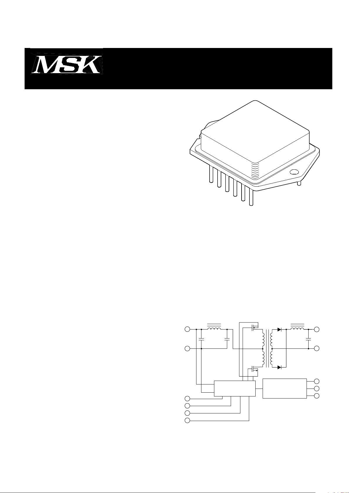
P W M
CURRENT MODE
CONTROLLER
ERROR AMPLIFIER
REFERENCE AND
ISOLATION
8
7
5
6
1
2
3
10
11
12
4
BLOCK DIAGRAM
4707 Dey Road Liverpool, N.Y. 13088
M.S.KENNEDY CORP.
(315) 701-6751
BBF2800S
SERIES
ISO-9001 CERTIFIED BY DSCC
20W
DC-DC
CONVERTERS
Rev. - 3/011
EXTERNAL CONNECTIONS
1
2
3
4
5
6
+INPUT
SHUTDOWN PLUS
CLOCK
ADJUST/COMP
-OUTPUT
+OUTPUT
12
11
10
9
8
7
-INPUT
TIMING 2
TIMING 1
CASE
-SENSE
+SENSE
Page 2

BBF2803S
ABSOLUTE MAXIMUM RATINGS
SPECIFICATIONS
ABSOLUTE MAXIMUM
RATINGS
INPUT VOLTAGE RANGE (Pin 12 to 1, 2, 3, 10 or 11) 0 - 50 Vdc
INPUT TRANSIENT (Pin 12 to 1) 80 V @ 50 ms
OUTPUT WITHSTAND (Pin 5 and 8 to 7, 6 or 4) 35 Vdc
OUTPUT CURRENT (Continuous) 5.5 Adc BBF2803S
4.0 Adc BBF2805S
1.9 Adc BBF2812S
1.5 Adc BBF2815S
TEMPERATURE, Storage –65
o
C, 150oC
TEMPERATURE, Pin Soldering 10s 300oC
NOTES: 1. Unless otherwise stated: TC = 25°, VIN = 28V, I
OUT
= I
MAX AMPS
2. Derate power linearly to zero from 125°C to 135°C.
3. Regulation measured between pin 8 and pin 7.
4. Recovery spec assumes that converter has been OFF for at least 500ms.
CAUTION: The internal substrate contains beryllia (BeO). Do not break the seal. If accidentally broken, do not crush, machine, or
subject to temperatures in excess of 850°C to avoid generating toxic fumes.
CAUTION
SPECIFICATIONS
BBF2803S
PARAMETER TEST CONDITIONS
1
MIN TYP MAX UNITS
STEADY STATE CHARACTERISTICS
INPUT VOLTAGE RANGE 16 28 40 Vdc
OUTPUT VOLTAGE VIN; min to max Vdc @ I
MIN
3.2 3.3 3.4 Vdc
OUTPUT CURRENT VIN; min to max Vdc 500 5500 mAdc
EFFICIENCY 66 %
OUTPUT RIPPLE VOLTAGE Bandwidth 10 kHz to 1MHz 20 50 mVrms
INPUT RIPPLE CURRENT Bandwidth 10 kHz to 1MHz 20 50 mArms
OUTPUT POWER
2
1.6 18.0 W
LINE REGULATION
3
VIN; min to max
3
2 20 mVdc
LOAD REGULATION
3
I
OUT
; min to max
3
1 15 mVdc
TEMPERATURE COEFFICIENT .01 %/°C
TEMPERATURE RANGE, case
2
–55 125 °C
QUIESCENT CURRENT I
OUT
= 0 A 35 40 mAdc
INHIBITED V
PIN5
; < 8 Vdc .09 1.25 2.5 mAdc
ISOLATION CHARACTERISTICS
(INPUT/OUTPUT/CASE)
LEAKAGE RESISTANCE (V
TEST
= 500Vdc) 100 MΩ
LEAKAGE CAPACITANCE (f = 10kHz) 50 pF
DYNAMIC CHARACTERISTICS
LINE STEP RESPONSE V
IN; TR
, TF = 10µs
VOLTAGE CHANGE VIN; 16 to 40 Vdc 300 mV
RECOVERY TIME (95%) 30 µs
WITH 100µF OUTPUT CAP
VOLTAGE CHANGE VIN; 16 to 40 Vdc 100 mV
RECOVERY TIME (95%) 100 µs
LOAD STEP RESPONSE I
OUT; TR
, TF = 10µs
VOLTAGE CHANGE I
OUT
; 50% to max Adc 1400 m V
RECOVERY TIME (95%) 40 µs
WITH 100µF OUTPUT CAP
VOLTAGE CHANGE I
OUT
; 50% to max Adc 300 mV
RECOVERY TIME (95%) 60 µs
START-UP OVERSHOOT VIN ; 0 to 40 Vdc 0 mV
SHUTDOWN DELAY V
PIN5
; > 10 Vdc to < 8 Vdc 220 500 µs
SHUTDOWN RECOVERY
4
V
PIN5
; < 8 Vdc to > 10 Vdc 30 60 mS
Rev. - 3/012
Page 3

SPECIFICATIONS
BBF2805S BBF2812S BBF2815S
BBF2805S BBF2812S BBF2815S
MIN TYP MAX MIN TYP MAX MIN TYP MAX UNITS
16 28 40 16 28 40 16 28 40 Vdc
5.00 5.05 5.1 12.00 12.05 12.1 15.0 15.1 15.2 Vdc
400 4000 190 1900 150 1500 mAdc
70 72 73 %
20 50 25 50 25 50 mVrms
20 30 20 30 20 30 mArms
2 20 2.3 23 2.2 22 W
5 50 5 50 10 50 mVdc
2 25 5 50 20 50 mVdc
.01 .01 .01 %/°C
–55 125 –55 125 –55 125 °C
35 40 35 40 35 40 mAdc
.09 1.25 2.5 .09 1.25 2.5 .9 1.25 2.5 mAdc
100 100 100 MΩ
50 80 85 pF
400 300 300 mV
30 40 40 µs
200 150 150 mV
250 250 250 µs
1400 800 800 mV
40 60 60 µs
500 280 280 mV
150 400 400 µs
000mV
220 500 220 500 220 500 µs
30 60 30 60 30 60 ms
PACKAGE THERMAL SPECIFICATIONS MIN TYP MAX UNITS
RESISTANCE, case to air 12 °C/W
TEMPERATURE RISE, junction to case 10 15 °C
Rev. - 3/013
Page 4

BBF2803S
TYPICAL PERFORMANCE
GRAPHS
0.0 6.0
OUTPUT CURRENT, I
OUT
(A)
10
12
14
16
18
20
LOW LINE DROP OUT
INPUT VOLTAGE, V
IN
(V)
2.0 4.0
10K 90K60K20K 30K 40K
INPUT VOLTAGE, V
IN
(V)
TIME, t (500µsec/DIV)
LOAD TRANSIENT RESPONSE 1000µF LINE TRANSIENT RESPONSE
EFFICIENCY CONTOURS
16
30
40
35
20
25
OUTPUT RESPONSE, X (UNITS/DIV)
OUTPUT CURRENT, I
OUT
(A)
4.4.55 1.1 2.2 3.3 5.5
SET POINT RESISTOR, R
SP
(Ω) TIME, t (5msec/DIV)
12
16
20
24
28
TURN ON THRESHOLD
TURN ON VOLTAGE, E
TO
(V)
TURN ON RESPONSE
100 200 400
FREQUENCY, f (Hz)
–100
AUDIO REJECTION
AUDIO REJECTION, A
V
(dB)
0
–20
–40
1K 2K 10K20K 100K
–60
–80
RESPONSE, X (UNITS/DIV)
3.3V
0V
0V
28V
V
OUT
V
IN
TEMP = 25°C
40%
50%
56%
60%
64%
66%
67%
68%
69%
66%
70%
INPUT VOLTAGE, V
IN
(V)
EFFICIENCY CONTOURS
16
30
40
35
20
25
OUTPUT CURRENT, I
OUT
(A)
TEMP = 125°C
40%
50%
60%
64%
66%
67%
68%
69%
70%
64%
INPUT VOLTAGE, V
IN
(V)
EFFICIENCY CONTOURS
16
30
40
35
20
25
OUTPUT CURRENT, I
OUT
(A)
4.41.1.55 2.2 3.3 5.5 4.41.1.55 2.2 3.3 5.5
TEMP =
–55°C
30%
40%
50%
54%
58%
60%
62%
64%
65%
66%
67%
INCLUDES 1000µF ON OUTPUT BUS
TIME, t (200µsec/DIV)
TIME, t (200µsec/DIV)
LOAD TRANSIENT RESPONSE 100µF
OUTPUT RESPONSE, X (UNITS/DIV)
OUTPUT RESPONSE, X (UNITS/DIV)
LOAD = 5.5A
LOAD = 5.5A
INCLUDES 100µF ON OUTPUT BUS
INCLUDES 100µF ON OUTPUT BUS
INCLUDES 100µF ON
OUTPUT BUS
TIME, t (100µsec/DIV)
LOAD TRANSIENT RESPONSE
OUTPUT RESPONSE, X (UNITS/DIV)
5.5A
5.5A
5.5A
2.75A
2.75A
2.75A
V
OUT
V
OUT
V
OUT
V
IN
16V
40V
V
OUT
I
OUT
I
OUT
I
OUT
1 V2 A
1 V2 A
100mV10V
1 V
10 V 2 V
2 A
NO OUTPUT BUS CAPCITANCE
VIN = 28VDC
I
OUT
= 5.5 Amps
OUTPUT DC
CURRENT RATING
TEMP = 25°C
Rev. - 3/014
Page 5

BBF2805S
TYPICAL PERFORMANCE
GRAPHS
0.0 5.0
OUTPUT CURRENT, I
OUT
(A)
10
12
14
16
18
20
LOW LINE DROP OUT
INPUT VOLTAGE, V
IN
(V)
1.0 2.0 3.0 4.0
10K 90K70K20K 30K 40K50K
INPUT VOLTAGE, V
IN
(V)
TIME, t (500µsec/DIV)
LOAD TRANSIENT RESPONSE 1000µF LINE TRANSIENT RESPONSE
EFFICIENCY CONTOURS
16
30
40
35
20
25
OUTPUT RESPONSE, X (UNITS/DIV)
OUTPUT CURRENT, I
OUT
(A)
3.2.4 .8 1.6 2.4 4
SET POINT RESISTOR, R
SP
(Ω) TIME, t (5msec/DIV)
12
16
20
24
28
TURN ON THRESHOLD
TURN ON VOLTAGE, E
TO
(V)
TURN ON RESPONSE
100 200 400
FREQUENCY, f (Hz)
–100
AUDIO REJECTION
AUDIO REJECTION, A
V
(dB)
0
–20
–40
1K 2K 10K20K 100K
–60
–80
RESPONSE, X (UNITS/DIV)
5.1V
0V
0V
28V
V
OUT
V
IN
TEMP = 25°C
30%
40%
50%
60%
68%
70%
63%
66%
71%
72%
73%
INPUT VOLTAGE, V
IN
(V)
EFFICIENCY CONTOURS
16
30
40
35
20
25
OUTPUT CURRENT, I
OUT
(A)
3.2.4 .8 1.6 2.4 4
TEMP =
125°C
30%
50%
60%
64%
67%
67%
69%
70%
71%
72%
73%
INPUT VOLTAGE, V
IN
(V)
EFFICIENCY CONTOURS
15
30
40
35
20
25
OUTPUT CURRENT, I
OUT
(A)
3.2.8 1.6 2.4 4
TEMP =
–55°C
40%
50%
55%
60%
64%
71%
66%
68%
70%
69%
INCLUDES 1000µF ON OUTPUT BUS
TIME, t (200µsec/DIV)
TIME, t (200µsec/DIV)
LOAD TRANSIENT RESPONSE 100µF
OUTPUT RESPONSE, X (UNITS/DIV)
OUTPUT RESPONSE, X (UNITS/DIV)
INCLUDES 100µF ON OUTPUT BUS
INCLUDES 100µF ON OUTPUT BUS
INCLUDES 100µF ON OUTPUT BUS
TIME, t (100µsec/DIV)
LOAD TRANSIENT RESPONSE
OUTPUT RESPONSE, X (UNITS/DIV)
4A
4A
4A
2A
2A
2A
V
OUT
V
OUT
V
OUT
V
IN
16V
40V
LOAD 4A
LOAD 4A
V
OUT
I
OUT
I
OUT
I
OUT
1 V1 A
1 V1 A
100mV10V
1 V
10 V 2 V
1 A
NO OUTPUT BUS CAPCITANCE
VIN = 28VDC
I
OUT
= 4 Amps
OUTPUT DC
CURRENT RATING
TEMP = 25°C
Rev. - 3/015
Page 6

BBF2800S SERIES
APPLICATION
INFORMATION
OUTPUT ADJUST / COMP
The output voltage of the BBF2800S may be adjusted from
90% to 110% of nominal value by the use of a 50KΩ potentiometer as shown. Adjustment beyond this range is possible
however certain characteristics of the converter such as but
not limited to input voltage range, efficiency, ripple and temperature performance will change. Characterization by the
user is recommended in such applications.
Adjust/comp (pin 4) may be driven by external circuitry
referenced to pin 8 (-output sense) if desired. Grounding pin
4 causes output voltage to increase (25% typically) while
driving pin 4 above 1.3 V causes output voltage to decrease.
Pin 4 may be driven through 10KΩ or more if connection of the
comp function is also required.
The comp function of pin 4 allows transient response and
phase margin to be tailored to suit a specific application. This
feature may be utilized by connecting a small (1-500 nf)
capacitor between pins 4 and 6 or 7. This is generally recommended when very large low ESR load capacitances are
used.
SHUTDOWN PLUS
Pin 2 is used for remote shutdown, output fault detection,
and/or setting the input voltage point at which the converter
will turn on as shown in the typical application diagram. No
connection to pin 2 is necessary for normal operation of the
converter. Pin 2 is referenced to pin 12 (-input).
Shutdown may be implemented by simply connecting pin 2
to an open collector logic output or switch rated at 2.5 mA, 25
Vdc or higher.
Input voltage turn on point is programmed with a single
resistor from pin 2 to 12. An input turn on/off hysteresis
(typically 3.5% of Vin) will be observed. This should be
considered when making or verifying set point adjustment.
The value of the setpoint resistor may be determined by the
following:
210 • 10
3
R = (±10% accuracy at 25°C)
E
TO
– 9.5
Set point temperature coefficient is typically +400ppm/°C.
Output fault monitoring is accomplished by observing pin 2
with a high impedance monitoring circuit. Pin 2 voltage drops
from over 10 V to below 1 V when a load fault causes the
converters fault protection circuitry to activate. It will remain
low for at least 100 mS and return high. If the load fault is still
present pin 2 will return low and the cycle will repeat. If there
is no input setpoint programming resistor already in place a
resistor > 400 KΩ from pin 2 to 12 will provide pin 2 pull down.
MULTIPLE CONVERTER SYNCHRONIZATION
Synchronized operation of up to three BBF2800S series
converters may be accomplished without external components. One unit selected to be the master is connected
normally with pin 10 grounded. The clock output pin 3 will
provide the sync signal for up to two slave units. The slave
units have pin 10 not connected and receive the clock signal
into pin 11. The clock signal lines may be shielded to prevent
radiation. A separate 50 ohm coax to each slave unit is
recommended in order to preserve signal integrity. Shield
ends should be connected to pin 12 of the nearest converter.
BBF2800S converters may also be synchronized to an
external 500 KHz (+/- 5%) frequency source driving pin 11 of
the converters. Pin 10 is not connected. The converters
synchronize to the positive edge of the frequency source
allowing a variety of wave forms (pulse, square, spike) to be
used. Pin 11 is internally capacitively coupled allowing unipolar or bipolar frequency sources to be used. The source should
have a waveform rise time of 20 ns or less and be capable of
driving at least 4 volts peak into each 50 ohm pin 11 input (50
volts peak max).
An externally synchronized unit may be used to synchronize
other (slave) units. The slave units may be used in turn to
synchronize other slave units from their pin 3 outputs. Each
“generation” of slave units has a delay (100-200ns typical)
from the unit that it is synchronizing to.
4 7 8
50KΩ
TYPICAL APPLICATION
The above diagram shows the remote sense feature which
reduces Vo errors due to the resistance of the conductors
feeding the load. This diagram also shows the connections for
non-synchronized operation (TIMING 1 and 2) as well as
output voltage trim, remote shutdown, fault monitoring, and
input voltage turn on point adjustment.
Rev. - 3/016
Page 7

The information contained herein is believed to be accurate at the time of printing. MSK reserves the right to make
changes to its products or specifications without notice, however, and assumes no liability for the use of its products.
Please visit our website for the most recent revision of this datasheet.
M.S. Kennedy Corp.
4707 Dey Road, Liverpool, New York 13088
Phone (315) 701-6751
FAX (315) 701-6752
www.mskennedy.com
NOTE: ALL DIMENSIONS ARE ±0.010 INCHES UNLESS OTHERWISE LABELED.
ESD Triangle indicates Pin 1.
BBF2812S
The above example is an industrial grade 12V single output converter
ORDERING INFORMATION
SCREENING
BLANK= INDUSTRIAL; E= EXTENDED RELIABILITY;
H= CLASS H; K= CLASS K
SINGLE OUTPUT
OUTPUT VOLTAGE
03=3.3V; 05=5V; 12=12V; 15=15V
NOMINAL INPUT VOLTAGE
GENERAL PART NUMBER
Rev. - 3/01
7
MECHANICAL SPECIFICATIONS
 Loading...